|


|
|

| Ask the Experts | ||||||||||||||||
|
||||||||||||||||
|
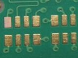
July 9, 2025 - Updated August 22, 2018 - Originally Posted Pad Missing ENIG Plating
Our fabrication drawing clearly specifies ENIG, so I think these boards should be either re-plated with ENIG or scrapped at the fabricator's expense. What do the experts say? S.M. |
||||||||||||||||
| Expert Panel Responses | ||||||||||||||||
|
My advice is to reject the boards. They were not manufactured to specification. They should be re-plated or scrapped at the fabricator's expense. Mixing finishes on the same board could compromise solder joint integrity.
Manufacturing Applications Specialist Cirtronics Corp. Mr. Bush has over 30 years of experience in electronics contract manufacturing. Major areas of expertise include through-hole, SMT, wave, and selective soldering.
As the co-chairman of the committee responsible for ENIG, rework of the boards post nickel plating is NOT allowed and is rejectable. The supplier needs to share with you the root cause for the skip plating, why the copper did not take catalyzation but would now take an OSP and be solderable. Additionally, given the source of free copper ions during plating, you should confirm that the ENIG plated pads are not exhibiting hyper corrosion. Unless these boards use super special material that is not available in a timely manner, I would reject them per the IPC 4552A.
President S T and S Testing and Analysis Gerald O'Brien is Chairman of ANSI J-STD 003, and Co Chairman of IPC 4-14 Surface Finish Plating Committee. He is a key member of ANSI J-STD 002 and 311 G Committees Expert in Surface finish, Solderability issues and Failure analysis in the PWA, PWB and component fields.
OSP should be OK as long as the Copper is precleaned and not too thick over the Gold.
Technical Sales Manager BLT Circuit Services Ltd Greg York has over thirty two years of service in Electronics industry. York has installed over 600 Lead Free Lines in Europe with Solder and flux systems as well as Technical Support on SMT lines and trouble shooting.
Either replating with ENIG completely or which will give in assembly reflow profile. Same time those pads. Must be exposed to.plate not to be covered by solder mask if so it's difficult and challenging rework by supplier. It's strange that how the supplier can miss out the pads which shows in Gerber as pads.
Engineer, Process Development Sanmina India Pvt ltd Engineering and Management oriented manufacturing background with a dedicated career experience of 19+ years involved in New Product Introduction, Product Engineering & study, Process development, SMT Engineering, Process Engineering, Industrial Engineering, Project milestone planning, Mass production planning and migration, Program management, Product quality Assurance and Document control analysis.
I would agree... Adding OSP would most likely be on the Nickel or Bare Copper. Assuming these are solder pads. I would request that Gold be final finish, or your soldering could be affected, especially when multiple thermal cycles are involved. Since they didn't ensure these were Au plated, they are most likely bare Copper.
Capital Equipment Operations Manager Specialty Coating Systems Rodney is currently Operations manager at SCS coatings, Global Leader in Parylene and Liquid Coating equipment. Rodney applies his BS in Computer Integrated Manufacturing from Purdue University, along with 20+ years of Electronic manufacturing and Equipment Assembly, to direct the Equipment business at SCS Coatings. "We provide unique, value added coating equipment solutions for our customers". Including conformal, spin and Parylene coating expertise.
Skipped pads can occasionally occur with ENIG, or other chemically deposited coatings (I've seen it with Immersion Ag, for instance). Re-plating the boards with ENIG is going to be pretty much impossible. It's your call as to whether to accept another coating on the skipped pads. If you believe that process compatibility or reliability will be impacted, you are correct to ask for them to be re-made. You have to weigh the risk of accepting the alternative coating against the time lost for re-fabrication and the potential impact on supplier relationship.
Process Engineer Astronautics Fritz's career in electronics manufacturing has included diverse engineering roles including PWB fabrication, thick film print & fire, SMT and wave/selective solder process engineering, and electronics materials development and marketing. Fritz's educational background is in mechanical engineering with an emphasis on materials science. Design of Experiments (DoE) techniques have been an area of independent study. Fritz has published over a dozen papers at various industry conferences.
I suggest maintaining the original ENIG is the required finish. While the skipped pads are all that appears to be an issues I would be leery of the rest of the plating. Regardless you paid for the gold plating and it should be consistent throughout. On a side note, in all my years I have never had a board house make this type of a recommendation. Poor judgement.
Director of Corporate Quality Assurance Delta Group Electronics Inc. Tod has been working in the Aerospace Electronics Industry for 25 years, beginning with 4+ years working for PCB fabricator ending as the Quality Manager and 20 years with Delta Group Electronics Inc. an AS9100 registered electronics contract manufacture. Currently position is Director of Corporate Quality Assurance.
No doubt in my mind that based on the photo, this board does not meet the spec as noted. Buying on price has its issues for sure but in this case the spec is clearly noted so these boards should be rejected and replace with ones that do meet specifications or else the spec should be changed.
President and Founder Fein-Line Associates Mr. Feinberg is a 52 year industry veteran and President and founder of Fein-Line Assoc, a consulting group serving the Global Interconnect and EMS industries.
If you apply OSP to the pads you have two different finishes, unacceptable by both IPC and customer drawing requirements I am sure. The fabricator should have caught this at ENIG plating and should have been able to resolve the issue or scrap the boards. The better question is why did the gold not plate? Is there a contamination issue inhibiting the gold process and this is further just identifying an under lying issue? I would highly suggest to scrap the boards.
Fellow Raytheon Mark has over 35 years of experience in electronics fabrication, quality, and reliability while working for Raytheon RMD, IEC Electronics, GE, Motorola, ORS, etc. He has most recently taken the role as a Fellow at Raytheon in Tucson, AZ; prior to that, he established IEC Electronics Analysis and Testing Laboratories (IATL), LLC in Albuquerque, NM, for electronics and material analysis testing in the military, medical, and industrial industries. His expertise includes PCB, PCBA, components, and analytical and electrical analysis techniques.
In regards to missing ENIG, I would require the supplier to provide you the ENIG boards you ordered. It is their responsibility to correct the error in their process.
Sr Field Applications Support Engineer Kester Inc. Mr. Kaminsky has 30+ years of circuit board soldering assembly experience along with a patent for wave solder VOC flux process.
Firstly, the specification clearly states ENIG, unless there is a written deviation, using OSP to cover the pads that were missed is not an option and I doubt anyone would sign off on that deviation considering risk. I would also have concerns with re-plating these boards with ENIG since there is a reason why they didn't plate in the first place. One likely cause could be Soldermask on pads or redeposit of contamination during the soldermask curing process. Either way, it would be expected that the pads wouldn't plate during a rework attempt as something was prohibiting it from plating in the first place. This then means a "scrubbing" process would be utilized to clear the pads of any contaminates. That in turn introduces other issues and risk. The clear answer, taking everything into consideration here, would be to sort and scrap the non-conforming boards at the suppliers expense.
Director of Quality / CLSSMBB FCT Companies Mr. Bock has worked in the Electronics Manufacturing Industry since 1996. He has extensive experience in the PCB manufacturing industry along with PCB Assembly. He has spent 6 years working in Southeast Asia.
It's the fabricators problem, not yours... return the entire batch as "rejected, does not meet spec".
President JSK Associates Based in. Northern California since 1971. Founded JSK Associates in 1979. Actively involved in soldering, cleaning, chemistries. 30 years experience in EOS/ESD control.
"Skipped" or missed pads can occur in the ENIG plating process. Normally it is caused by an issue with catalyzation so that nickel will not plate properly on those particular pads. The skipped pads may have trace amounts of the catalyst metal, nickel and/or gold on the surface. It would be difficult to plate those pads with ENIG without potentially damaging the ENIG finish on other pads. It is possible to strip the ENIG coating off of the circuit boards through some aggressive chemical processing, but that is time consuming and can potentially damage the copper circuitry. OSP coating of the "skipped" pads is likely an easy solution for the PCB fabricator. If you specify ENIG, then I would recommend not accepting OSP. If you had a mixed finish of OSP and ENIG on the same circuit boards then the solder joints and their corresponding metallic bonds would me mixed as well. S oldering to OSP forms copper/tin intermetallic layers while soldering to ENIG forms nickel/tin intermetallic layers. I suggest having the boards built again with the ENIG finish properly applied to all of the pads.
Field Applications FCT Assembly Tony has worked in the electronics industry since 1994. He worked as a process engineer at a circuit board manufacturer for 5 years. Since 1999, Tony has worked for FCT Companies as a laboratory manager, facility manager, and most recently a field application engineer. He has extensive experience doing research and development, quality control, and technical service with products used to manufacture and assemble printed circuit boards. He holds B.S. and M.B.S. degrees in Chemistry.
The most common reason for this to occur is that the fabricator could have micro-etch solution remaining in the holes. If a pad is connected to that hole the ENIG plating will skip even if the contact is through an inner layer of the board. You might suggest your fabricator take the following actions if they have not done so already: 1) make sure there are no residues in the holes, 2) improve rinsing after micro-etch, 3) increase time in the activator, 4) increase activity in the Ni-bath, and 5) most important check the rinsing of the holes. Above all I would suggest your fabricator should not apply OSP to the pads with missing plating and should instead either re-pate with ENIG or scrap the boards.
General Manager Nordson SELECT Carlos Bouras is the General Manager of Nordson SELECT and has over 30 years of experience in the electronics manufacturing industry. Carlos's expertise is in process engineering, product development and manufacturing operations. For the past 15 years Carlos has focused specifically on automated assembly issues and is the holder of several US patents for non-contact dispensing and precision dispensing of adhesives for the packaging of microprocessor devices.
If the pads were not plated because of the design of the board, then OSP is a good solution. Note that:
Director of Sales and Marketing Sierra Circuits Amit Bahl started to work at Sierra Circuits in 2006 where he formed strong relationships with his customers working with them on flex PCBs, HDI, controlled impedance, etc. In 2009, he was promoted Director of Sales and Marketing.
To provide a flat pad, nickel is plated to the copper at a thickness of approximately 150 microinches (not 150 microns). Nickel oxidizes fairly quickly, so a very thin layer of gold (3 to 5 microinches) is subsequently plated over the nickel (not underneath as others have said) to prevent it from oxidizing. ENIG is preferred by some for that reason; the solderability remains excellent for years. The purpose of the nickel in ENIG is to provide a barrier between the copper pads and the gold. If the nickel is skipped and the gold is plated directly to the copper, a reaction will occur and over a very short time the copper will eat through the gold and can even appear on the surface as an "orange pad". You cannot solder to this pad without physically removing these oxides first. Chemical stripping can be done, but not without some collateral damage to other features, including the solder mask and the unprotected via walls. It is also very difficult to clean away 100% of the stripper, some always remains behind. During the soldering process, 100% of the 3 to 5u inches of gold on the top is immediately dissolved into the molten solder; no solder joint is formed with the gold. The underlying nickel is then exposed, and some of the nickel will dissolve into the molten solder, but no-where near all 150u inches of it. Your intermetallic layer is then made of the dissolved nickel into the solder alloy; you solder to the nickel barrier. The rate of dissolution of the nickel into molten tin/lead solder is 10 times slower than the rate of dissolution of copper into that same solder. At reflow temperatures, it takes a little bit longer to form a good IMF with nickel than it does with copper. Consider then, attempting to solder a PCB that has some pads with no nickel, some with, and some that may or may not have nickel under the gold. For those pads that meet the IPC 4552 standard, the gold will be immediately absorbed, and if the nickel is at least 100 u inches thick, no copper oxides will have formed, and the nickel should form a good IMF with the molten solder. For those pads that never had benefit of nickel, but are only exposed copper with a thin OSP coating that was probably applied several days after the problem was discovered and is subsequently oxidized to the level of a 1910 Lincoln penny, well, the chances of forming a good IMF between the solder and the copper is sort of like maybe, but probably not. When soldering, as others here have stated, some IMFs are going to form more than others, and while some IMF is usually enough, the fact is at least SOME of those pads that APPEAR to have plated over just fine and are actually skipped or nearly skipped and yet are covered with gold with some degree of nickel oxide barrier under the gold, who knows? You simply cannot solder to an oxide, once formed. Flux will not remove these types of oxide barriers effectively. With ENIG, a fabricator has to keep many, many process parameters under perfect control before, during, and after nickel plating, and even more so when doing the final gold plating. It is quite obvious that some or many things went wrong with this lot. So Tony Lentz and Jerry Karp gave you good advice; scrap the entire lot and tell the fabricator to replace them, and make sure the fabricator does not take the bad lot back and rework them and sell them to you later. Look for another fabricator who has some proven experience in ENIG plating. They have to run a very tight ship to plate ENIG properly (and any other finish as well, for that matter). A really good IPC-certified board shop can show you complete process control metrics, and the IPC has excellent standards for performing a PCB fabricator audit.
Advanced Engineer/Scientist General Dynamics Richard D. Stadem is an advanced engineer/scientist for General Dynamics and is also a consulting engineer for other companies. He has 38 years of engineering experience having worked for Honeywell, ADC, Pemstar (now Benchmark), Analog Technologies, and General Dynamics.
|
||||||||||||||||
| Submit A Comment | ||||||||||||||||
|
Comments are reviewed prior to posting. You must include your full name to have your comments posted. We will not post your email address. |


|
Free Newsletter Subscription
Circuitnet is built for professionals who bear the responsibility of looking ahead, imagining the future, and preparing for it. Insert Your Email Address |
|


|