|
|
|
|
|
|
|
|
|
|
|
|
| Ask the Experts | ||||||||||||
|
||||||||||||
|
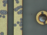
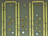
February 6, 2018 - Updated January 24, 2010 - Originally Posted Cause of Unusual Contamination?We have 40 PCB assemblies with unusual contamination. Do you have any ideas what the contamination is, and what caused it?
M. G. |
||||||||||||
| Expert Panel Responses | ||||||||||||
|
It is impossible to figure out what this is without more data. It looks like moldew or mold, or corrosion caused by splashes of something. My suggestion is to get an analytical lab, equipped with an IR microscope to take a look at the spots on the board. The resolution can be very high. Also need to figure out if it's "organic" or inorganic. Just need more data. Also, would be helpful to know stirage history, manufacturing process steps, etc. Sorry I can't be more helpful...but a photo is just not enough. Again, I'll be happy to chat with the person, gratis to help solve the problem.
Chairman Polyonics, Inc. Jim Willimas is a PhD Chemist in Polymers and Materials Science. He specialize in printing, cleaning, inks, and coatings used in electronics manufacturng operations. Williams has more than 30 years experience.
Unusual contamination indeed! The most obvious characteristic of this contamination is its linearity. Next, it apparently stops and starts where the mask begins. It looks to be corrosion of some kind ~ but that is a difficult call to make from an image. Under high magnification you may be able to better see what you have. Keep in mind, that gold is very resilient, and that chances are that "corrosion" is also present beneath the mask. Linear contamination theoretically could come from anywhere on the production line. It could be a dripping action, however, as it appears to end and begin anew as the mask comes and goes it strikes me that the source is not likely to be in the "downstream" assembly process. Do you have any other lots of these substrates to compare downstream processing versus as received? I suspect your root cause may be well upstream of assembly with your substrate suppler.
Vice President Kyzen Corporation Mr. Forsythe is a recognized expert in cleaning chemistries and processes. Tom has a Bachelor's in Applied Mathematics & Engineering from the US Naval Academy. He is well published in both the industry trade magazines. Tom has spent the last 14 years with Kyzen Corporation.
It looks like a splatter of something on the underlying metal that kept the (what appears to be) gold plating from seeding and plating. Note that there is no splatter on the substrate outside of the circuit so whatever it was washed or dissolved off subsequent to the plating process. Perhaps an analysis of the material that appears in the center of the discolored areas might solve the mystery. In my opinion the culprit appears to be lack of process detail just before gold plating
President and Founder Fein-Line Associates Mr. Feinberg is a 52 year industry veteran and President and founder of Fein-Line Assoc, a consulting group serving the Global Interconnect and EMS industries.
Unusual contamination? The photos show what appear to be contamination below the soldermask from the etch process not properly rinsed. The pockets of contamination (typically sulfuric acid) rarely show up as an incoming board but run it over a wave or selective soldering process and these corrosion attacks of the base copper below the soldermask or occasionally through pin holes in the mask will appear.
President/Senior Technical Consultant Foresite Mr. Munson, President and Founder of Foresite, has extensive electronics industry experience applying Ion Chromatography analytical techniques to a wide spectrum of manufacturing applications.
Without more details, it is difficult to assess for certain what the issues are. It looks as though solder balls had reflowed onto the Au areas. My first action would be to look to see if these boards were washed due to misprints. Misprint cleaning often leaves stray solder balls which could coalesce when reflowed later. The second thing I would look at is the printing process and, most importantly, the under stencil cleaning process. The under stencil cleaning can sometimes smear solder paste across the bottom of the stencil allowing the solder to contaminate subsequent boards. In both of these cases, the solder particles are very difficult to see prior to reflow. After reflow, they will wet to the Au surface and become readily apparent. The third area to look at would be solder spatter during the reflow process. A slow ramp in the preheat stage of the reflow process will help to slowly volatilize the flux and minimize the potential for splattering.
Product Manager, Advanced Assembly Materials Indium Corp. Timothy Jensen is the Product Manager for Indium Corporation's PCB Assembly Materials and has spent over a decade troubleshooting and optimizing SMT process lines. Having worked directly on hundreds of surface mount lines, and building thousands of different products, Tim understands each customer's unique requirements, and tailors Indium's products and services to meet or exceed those needs.
Solder seems to have been trapped in the vias. During subsequent reflow, the solder inside the via will melt and can outgass causing it to spatter and fall on the gold pads.
Technical Manager - Europe Indium Corp. Currently with Indium Corporation and responsible for technology programs and technical support for customers in Europe. Over 15 yrs experience in SMT, Power, Thermal & Semiconductor Applications. Masters Degree in Industrial Engg, State University of New York-Binghamton.
This contamination appears to be due to particles of solder paste being present across the surface during reflow. These have melted and spread to cause these patches of solder. Perhaps this has been a badly printed PEC which was not washed off properly.
Principal Engineer - CMA Lab BAE Systems Bryan Kerr has 35 years experience in providing technical support to PEC assembly manufacturing. His experience ranges from analysis of materials and components to troubleshooting and optimizing, selecting reflow, cleaning, coating and other associated processes.
The stain on the conductive traces appears to be an acidic or alkaline liquid that was dripped and left onto the traces. Question, did you use selective soldering on this assembly? If so, were you using a water soluble flux?
CTO Kyzen Corp. Mr. Bixenman is the CTO for Kyzen Corp. Kyzen Corp. is a leading provider of engineered cleaning fluids for high technology manufacturing environments.
Pore corrosion. I assume this is gold over nickel plating structure. Depending upon the duration, could indicate elevated levels of corrosive gases.
CEO & Managing Partner DfR Solutions Dr. Hillman's specialties include best practices in Design for Reliability, strategies for transitioning to Pb-free, supplier qualification, passive component technology and printed board failure mechanisms.
This looks more like metal migration through the gold plating - Iwould contact the PCB supplier. If this a TH only board, the solder coming froman improper cleaning of the stencil is out of the question.
Engineering and Operations Management Independent Consultant Georgian Simion is an independent consultant with 20+ years in electronics manufacturing engineering and operations.
Contact me at georgiansimion@yahoo.com. To me it looks like chemical attack of lower layer through the pin holes in the top layer. A close examination at high magnification would confirm. Integrity of top layer is a suspect.
Head-Quality Astra Microwave Products, Hyderabad, AP India Holds Degree in Engineering, started off as Scientist/Engineer in ISRO (Indian Space Research Organization) in Quality Assurance of Space hardware Electronics Production. Worked in the area of Parts, Material and Process; DPA, FA and Process Qualification for space and ground hardware. Later moved into Private sector and worked in the area of Quality Management Systems & ISO 9001 certification. Currently hold a position as Head-Quality in RF/Microwave Product manufacturing for Defense and Aerospace segment.
Reader Comment
How was the area masked off? Might it be contamination contained within the masking substance? Seems as if the area is concentrated within the center of the mask area.
Pat Goodyear, Pacific Gas and Electric
Reader Comment
The spots all look pretty much the same size except where multiple hits (dots) glom together. I would not think they were caused by splattering, or drippings, or contaminates. Although I am not an expert on these things.
T.T.
Reader Comment
I agree with the responses from Bran Kerr and Tim Jensen.
This condition is contamination due to stray solder paste which was most likely deposited on the gold surfaces as a result of poor stencil underside cleaning or residual solder spheres left behind after cleaning a misprint.
As previously mentioned, the spheres are not generally visible with the naked eye until they have reflowed and wet the gold.
Another example of this is Figure 10-3 from IPC-A-610D.
D.S.
I would agree with the uniform wetting and sizes being from solder powder and probably from poorly cleaned screens spreading the powder over the bottom of the stencil then picking up on the PCB and reflowing.
Technical Sales Manager BLT Circuit Services Ltd Greg York has over thirty two years of service in Electronics industry. York has installed over 600 Lead Free Lines in Europe with Solder and flux systems as well as Technical Support on SMT lines and trouble shooting.
Reader Comment
Without examination it's hard to be certain, but we did have an assembly that exhibited the exact same appearance as your photos. Root cause was determined to be an insufficient rinse during bare board manufacturing. Boards looked normal upon incoming inspection, but contamination appeared after reflow.
Jeffrey Myers, Surmotech, LLC.
Reader Comment
I'll add another vote for solder splatter due to poor stencil cleaning
Dave Hillman, Rockwell Collins
|
||||||||||||
| Submit A Comment | ||||||||||||
|
Comments are reviewed prior to posting. You must include your full name to have your comments posted. We will not post your email address. |


|
Free Newsletter Subscription
Circuitnet is built for professionals who bear the responsibility of looking ahead, imagining the future, and preparing for it. Insert Your Email Address |
|
|
|
|
|
|
|
|