|


|
|

| Ask the Experts | ||||||||||
|
||||||||||
|
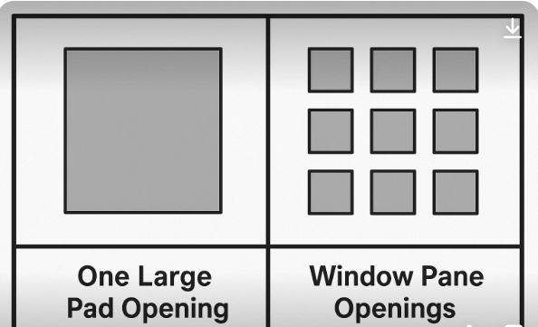
April 30, 2025 - Updated April 21, 2025 - Originally Posted Stencil Pattern for LGA Power PadWe are experiencing difficulties reliably soldering the large ground pad on land grid array (LGA) packages using a single large window in the stencil. Should we use multiple smaller windows when dispensing solder paste for the center ground pad? The MFG data sheets do not provide options for using a multi-window paste stencil. Can you give a reasonable rule to follow, regardless of the size of the LGA ground pad, when using multiple smaller windows in the stencil? J.M. |
||||||||||
| Expert Panel Responses | ||||||||||
|
This does not sound like a solderpaste volume issue but a function of thermal management and the ground plane will sink away the heat just enough to not allow the ground to transition into liquidous solder and form the joint. Call me or my staff and we can help.
President/Senior Technical Consultant Foresite Mr. Munson, President and Founder of Foresite, has extensive electronics industry experience applying Ion Chromatography analytical techniques to a wide spectrum of manufacturing applications.
Yes, using multiple smaller stencil apertures (often referred to as a "window pane" or "segmented" pattern) for the center ground pad on LGA packages is generally recommended over a single large aperture. This approach helps to mitigate several common soldering issues such as voiding, insufficient solder spread, Solder Beading and solder paste slump. Recommended Practice: Based on IPC-7093 (Design and Assembly Process Implementation for Bottom Termination Components) and SMTA best practices, a segmented stencil design should be used for LGA thermal pads. Here's a general guideline: Rule of Thumb:
Why It Works:
Note: Although MFG datasheets may not show segmented aperture options, many manufacturers and contract assemblers have adopted this approach based on field experience and IPC recommendations.
Engineering Director / Master IPC Trainer (MIT) AMMSA Solutions More than 20 years of technical experience in the electronics industry in roles ranging from Process & Project Engineer to engineering manager and Technical Applications Engineer for Latin Americas. IPC Master Trainer, International speaker and consultant.
It’s a good idea to divide the large ground pad into smaller stencil openings. A single large opening often traps flux and causes solder voids. For LGA ground pad, don’t use one big opening in the stencil. Instead, break it into smaller square or rectangular openings (around 1–1.5 mm in size), spaced slightly apart. Aim for the total paste to cover about two-thirds of the pad area. This works for small and large pads, just adjust the number of windows to fit the size. The goal is to let gas escape during reflow and avoid big solder voids.
CTO Cybord Electronic and Mechanical Engineer with 25 years experience in technology development. CTO of Cybord, developing electronic component authentication technology using deep-tech visual inspection and big-data. Author of a book and 24 papers.
This is not an uncommon issue at all. If you have access to a 3-D paste inspection system, you will see that the center of the large window gets “scooped out” and so the paste volume printed is much less than expected. The thinner the stencil thickness, the worse this effect gets. Using an array of smaller windows is a good work-around. There is a minimum “web width” between the windows that will be mechanically durable, and this web width will grow somewhat as the window “pane” size increases. You want to keep the “percent open area” within the overall window as high as possible, while keeping the pane dimensions small enough to avoid scooping. Typically, a pane dimension of 2mm or 2.5mm is fine, and you may be able to go a bit larger. You should be able to keep the webs between panes down to 0.25mm or so and still have acceptable mechanical strength. In addition to using window panes, do optimize your squeegee pressure. Don’t use any more pressure than is necessary to reliably clear the top surface of the stencil of paste, as scooping increases with increasing pressure.
Process Engineer Astronautics Fritz's career in electronics manufacturing has included diverse engineering roles including PWB fabrication, thick film print & fire, SMT and wave/selective solder process engineering, and electronics materials development and marketing. Fritz's educational background is in mechanical engineering with an emphasis on materials science. Design of Experiments (DoE) techniques have been an area of independent study. Fritz has published over a dozen papers at various industry conferences.
We recommend breaking up the solder paste print on large power pads into multiple bricks using a window pane type design. A good rule of thumb is to ensure the area of coverage of the solder paste on the pad is 65-75%. The width of the window pane "webs" should be kept small (10-15 mils). The number of window panes should also be minimized, as too many window panes (too many webs) can lead to voiding in the solder joint. Some stencil providers can design a recommended set of stencil apertures to optimize soldering for LGA power pads.
Field Applications FCT Assembly Tony has worked in the electronics industry since 1994. He worked as a process engineer at a circuit board manufacturer for 5 years. Since 1999, Tony has worked for FCT Companies as a laboratory manager, facility manager, and most recently a field application engineer. He has extensive experience doing research and development, quality control, and technical service with products used to manufacture and assemble printed circuit boards. He holds B.S. and M.B.S. degrees in Chemistry.
The industry recommends a window pattern that provides 50 to 70% pad coverage. This pattern will remove the “floating effect” and will allow for an outgassing path to minimize surface voiding.
Senior Manufacturing Engineer Northrop Grumman Edithel is a chemical engineer with 20 year experience in manufacturing & process development for electronic contract manufacturers in US as well as some major OEM's. Involved in SMT, Reflow, Wave and other assembly operations entailing conformal coating and robotics.
The window pattern on the stencil is one way to apply solder paste to the large ground areas beneath components. Each widow opening in the stencil will allow a smaller amount of solder as opposed to a larger area which could lift the component vertically and interfere with the solder joints around the periphery of the component.
As can be seen these are an example of windowpane openings. The other item of concern is any open via holes beneath the component(s) as this could create an outgassing which could impact solder joints around the periphery of the component. These stencil openings can be arranged in such a fashion as to not impact any vias beneath the component which would result in acceptable solder joints. As for the physical sizes, I found the following as a guide, but it all depends upon the physical component size and the layout on the board itself. Usually, no smaller than 0.3 mm x 0.3 mm to ensure good paste release, however, keep in mind the thickness of the stencil, thicker the stencil results in more paste being deposited.
Vice President, Technical Director EPTAC Corporation At EPTAC Corporation, Mr. Lambert oversees content of course offerings, IPC Certification programs and provides customers with expert consultation in electronics manufacturing, including RoHS/WEEE and lead free issues. Leo is also the IPC General Chairman for the Assembly/Joining Process Committee.
Without knowing all the details of your process, type of paste, stencil thickness, board finish, it is hard to determine the best approach. However- With most LGA pads especially larger ground pads, you need a means of out gassing which would prevent large voids. The multiple window pane is the most popular used. The number of panes will depend on a variety of factors including those I listed above. Having a robust oven profile is also critical. Your best bet would be to design a D.O.E. and experiment with a non-production PCB.
Manufacturing Applications Specialist Cirtronics Corp. Mr. Bush has over 30 years of experience in electronics contract manufacturing. Major areas of expertise include through-hole, SMT, wave, and selective soldering.
You should use “window pane” design- essentially breaking up in smaller pads. You should have gaps between different “windows” to endure 50 to 70% coverage. This will prevent tilting and floating of LGA which happens if you provide 100% coverage. In addition, window pane coverage will also reduce voids significantly in LGA thermal pads. For additional details please refer to IPC 7093 design and assembly guidelines for BTC that I initiated and chaired for over a decade.
President Ray Prasad Consultancy Group Ray Prasad is the founder of Ray Prasad Consultancy Group which provides teaching, consulting and technical expert services in tin-lead and lead free technologies using SMT, BGA, BTC, fine pitch and through hole components. Mr. Prasad is a long time member of IPC, and is currently the chairman of BGA committee IPC-7095 "Design and Assembly Process Implementation for BGA" and Co-Chairman of recently created IPC-7093 "Design and Assembly Process Implementation for Bottom Terminations" surface mount Components (BTCs) such as QFN, DFN and MLF.
|
||||||||||
| Submit A Comment | ||||||||||
|
Comments are reviewed prior to posting. You must include your full name to have your comments posted. We will not post your email address. |


|
Free Newsletter Subscription
Circuitnet is built for professionals who bear the responsibility of looking ahead, imagining the future, and preparing for it. Insert Your Email Address |
|


|