|


|
|

| Ask the Experts | |||||||
|
|||||||
|
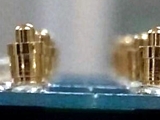
March 2, 2026 - Updated January 24, 2017 - Originally Posted What Is Causing Slanted Pins After Reflow
What should I do to prevent this. My stencil thickness 5 mils. J.A. |
|||||||
| Expert Panel Responses | |||||||
|
Due to the rheology of solder paste and density of the component you might experience the pogo pin to float during reflow causing some pogos to become slanted. Try the following: First, decrease the amount of solder paste deposited by decreasing pad aperture, workmanship standards could be affected if aperture is decreased too much. Second, if your SMD placement machine can be adjusted, increase placement force to secure component into the solder paste. Third, design a small tooling to keep pogos straight during reflow.
Senior Manufacturing Engineer Northrop Grumman Edithel is a chemical engineer with 20 year experience in manufacturing & process development for electronic contract manufacturers in US as well as some major OEM's. Involved in SMT, Reflow, Wave and other assembly operations entailing conformal coating and robotics.
The Pogo pins appear to be surface mounted and once the solder reflows and expands the components or pins will float on the molten solder. To keep the pins aligned I would suggest a template or fixture to hold the pins in place. If the pins were mounted into a fixture upside down, the paste could be screen onto the bottoms of the pins and the board could be aligned and placed over the pins and then processed through a reflow over to make the connection to the board. Once reflowed and the solder has solidified, then the fixture board could be removed and all the pins would be in alignment. The intent is to secure the pins prior to reflow.
Vice President, Technical Director EPTAC Corporation At EPTAC Corporation, Mr. Lambert oversees content of course offerings, IPC Certification programs and provides customers with expert consultation in electronics manufacturing, including RoHS/WEEE and lead free issues. Leo is also the IPC General Chairman for the Assembly/Joining Process Committee.
It sounds like the thin PCB is bowing slightly during reflow. Have them check to see if the pins bowing are in the same area/pins. A reflow fixture should help in eliminating this problem.
President and Founder Contract Manufacturing Consultants, Inc. Robert Fried helps leading electronics OEM's develop world-class sourcing strategies for PCBA, cables, precision metals, plastics, modules and complete end-products. Other service areas are supplier risk assessment, comprehensive outsource ...
If you have a mating connector, it is quite possible you can pull the mating sockets out and use the empty mating connector body as a reflow fixture (a pin holder) to hold the pins in place, or at least to use as a drill guide to make a mating connector using standard FR-4 material. Whatever you use as an alignment fixture should make contact with the PWB, but just perhaps in one spot on each end and one spot on each side to ensure the pins are as perpendicular to the surface as possible. This may be all that is needed to hold them perpendicular. If there is no danger of either the mating connector or the board pins reflowing together, (gold on gold), then I would think a mating connector that can take the reflow temperatures would make a perfect alignment tool, as it would provide a snug fit. The way to do it then would be to place the pins into the mating connector and turn the whole thing upside down and place all of the pins into the board and just leave the mating connector on until after reflow. If all of the pins are pushed all the way down into the mating tool, then they should be perfectly aligned. However, they will be perfectly aligned with respect only to the surface of the small, thin PWB. If the board is undergoing serious warping during reflow, then all of the pins will be slanted. However, the fix for that is to glue a thin piece of FR-4 material on the back side. This may or may not keep the PWB flat through reflow.
Advanced Engineer/Scientist General Dynamics Richard D. Stadem is an advanced engineer/scientist for General Dynamics and is also a consulting engineer for other companies. He has 38 years of engineering experience having worked for Honeywell, ADC, Pemstar (now Benchmark), Analog Technologies, and General Dynamics.
Reader Comment
From the photo, it appears that you have convex solder fillets. I was able to resolve a similar issue by increasing the diameter of the PCB pads and adjusting the size of the stencil apertures.
Rick Kompelien, Benchmark Electronics, Inc.
You need just enough solder to form a sufficient fillet at the base of the pin. Given a large enough PCB pad surface, the extra solder will wet outwards leaving a concave fillet and just enough solder underneath the part to form the intermetallic layer. This is a PCB design issue - increasing the pad size will allow for proper formation of solder fillets. If you can't get the PCB design changed, you could try reducing the solder volume with a thinner stencil or smaller apertures.
Principal Product Engineer Benchmark Electronics, Inc. 30+ years of experience working with electronic and electro-mechanical manufacturing and design (medical, automotive, military, computer, and industrial controls). Military veteran - served as a Combat Engineer with the United States Marine Corps.
|
|||||||
| Submit A Comment | |||||||
|
Comments are reviewed prior to posting. You must include your full name to have your comments posted. We will not post your email address. |


|
Free Newsletter Subscription
Circuitnet is built for professionals who bear the responsibility of looking ahead, imagining the future, and preparing for it. Insert Your Email Address |
|


|