|


|
|

| Ask the Experts | |||||||
|
|||||||
|
October 24, 2025 - Updated July 15, 2015 - Originally Posted Calculating PCB Hole DiametersOur bare boards are typically .065" thick. How can we calculate the hole diameter for connector pins if the board thickness increases to .150"? P.N. |
|||||||
| Expert Panel Responses | |||||||
|
Many manufacturers have the capability of producing boards with a via aspect ratio of 10:1. If we apply this specification to your .150" board, the smallest through-hole diameter should be .015 inches. Your board shop should be able to provide more information on your design.
Senior Manufacturing Engineer Northrop Grumman Edithel is a chemical engineer with 20 year experience in manufacturing & process development for electronic contract manufacturers in US as well as some major OEM's. Involved in SMT, Reflow, Wave and other assembly operations entailing conformal coating and robotics.
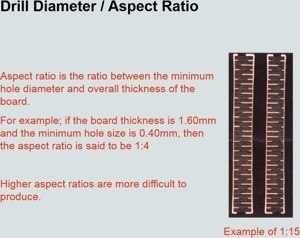
Aspect ratio is the ratio between the minimum hole diameter and overall thickness of the board. For example; if the board thickness is 1.60mm and the minimum hole size is 0.40mm, then the aspect ratio is said to be 1:4 according to IPC, however when you change to a ticker PCB like you are, you will want to start reduce this aspect ratio, if the product is laid out for wave solder, as you will experience hole fill issues with this Aspect ratio. In most cases you should not go below the aspect ratio 1:15. Higher aspect ratios are more difficult to produce at PCB fabrication.You can refer to the attached images of a PCB DFM guidelines.
Process Engineering Manager - Electronics Altech UEC, South Africa Currently with Altech UEC and responsible for technology road map in PCBA electronic manufacturing and technical support for PCBA electronic manufacturing for Altech UEC and its JDM's. Over 7 years in SMT, Radial Insertion, Wave solder & Test Applications.
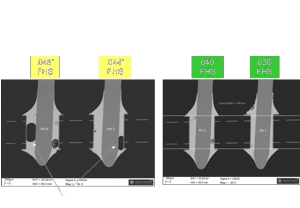
Pin to Hole ratio is important in Intrusive Reflow. The attached shows Pin to hole ratio ranging from .52 to .69 for .063" thick board. .63 and .69 give acceptable results while .52 and .56 leaves some voiding. Same pin to hole seem to apply for .093 thick board. Sorry can't help with .150" thick board.
Vice President Technology Photo Stencil For over 18 years, Dr. Coleman has been the vice president of technology for Photo Stencil, working closely with customers to understand their printing requirements. His efforts have resulted in several new stencil products.
Reader Comment
For the first part of the question you could check with your Assembly house. For the second part of the question you should check with your Fab house. Since we can do almost anything on a computer screen these kinds of 'questions and answers' should be based on trying to design a board using industry standard DFM guidelines to help keep the cost down. Other sources for answers would include IPC Standards and the component mfg. datasheets. Here are my two answers;
Don Lamothe, PCB Designer, Hudson NH USA
1. The minimum hole size for a component pin would be based on the size of the pin going into the hole, usually without regard to the thickness of the board. Other factors that would impact the minimum hole size would be how the board is being assembled (by hand vs. machine), the number of pins on the component (more pins require larger holes for tolerance), pin size tolerance, pin location tolerance, etc.. There are more answers to these kinds of questions then you can imagine. Try goggling "what is the minimum hole size for a component lead in a PCB" and you'll see what I mean. The best answer is to ask your PCB Assembly House since they're responsible for soldering the parts to the board. Make life easy for them and you'll keep the cost of the board down. 2. The second half of the question seems to refer to the minimum hole size for a .150" thick board. Now we need to consider what is called 'aspect ratio'. This is the "board thickness/minimum hole size". My answer here is based on mechanically drilled holes. If you need smaller holes, then Laser Drilling comes into play and that can be expensive. If the hole is too small it is difficult (or impossible) to guarantee plating in walls of the hole all the way down through the thickness of the board. The thicker the is the larger the hole needs to be. All PCB Fab houses should be able to handle a 6:1 aspect ratio (if yours can't, find a new Fab house). In a .065" thick board this would be approximately .011". In a .150" thick board this would be .025". Some Fab house can handle an aspect ratio as small as 10:1. In a .065" thick board this would be .0065" and in a .150" thick board it would be .015". For this question you should ask your Fab house for their minimum capabilities. Make life easy for them and you'll keep the cost of the board down. Reader Comment
I agree with the comments by different experts in the Field. Fab Capability and Economics play an important role in decision making while designing PCBs to meet special & Specific requirements within the Guidelines for Design & Manufacture as stipulated in IPC Standards.
Ranganath Mandayam, TQM Consultancy
Reader Comment
A decent bare board shop should be able to do 12:1 or better. When I worked in a bare board shop in the United States about 4 years ago, we routinely plated 16:1 aspect ratios. This is a real world number for medium volume, not marketing hype. Since then I have toured other plants that claim even higher ratios. There are limitations at this aspect ratio. HASL can not be used. Current density becomes more important. Talk to prospective board suppliers.
Tom Guinan, Axiom Electronics
|
|||||||
| Submit A Comment | |||||||
|
Comments are reviewed prior to posting. You must include your full name to have your comments posted. We will not post your email address. |


|
Free Newsletter Subscription
Circuitnet is built for professionals who bear the responsibility of looking ahead, imagining the future, and preparing for it. Insert Your Email Address |
|


|