|


|
|

| Ask the Experts | |||||||
|
|||||||
|
March 30, 2026 - Updated January 9, 2020 - Originally Posted Causes of Annular Ring Dewetting
What are the reasons for this phenomena? What process parameters, both PCBA manufacturing and bare board manufacturing are critical? If this is related to bare boards manufacturing, how can we discover the failure before the PCBA assembly process? R.L. |
|||||||
| Expert Panel Responses | |||||||
|
Require: (1) an IPC/JEDEC J-STD-003 solderability witness sample (float or dip) with each shipment. (2) an extra pallet @ N/C for pre-assembling solderability testing (e.g., a bare pallet rejected at ET).
President Circuit Connect, Inc. Bob has been in PCB design and fabrication since 1976. He has held elected positions with the SMTA, is a member of the MSD Council, has served as a committee member for various IPC standards and is a Certified IPC Trainer.
Need some clarification and possibly pictures if possible to accurately advise. In my experience actual dewetting has almost always been contributed to contamination in either the PCB, component or solder. Most dewetting issues I have seen were incorrectly dispositioned and were actually nonwetting defects. For any wetting issue, either nonwetting or dewetting, I suggest performing a JSTD solderability test on the PCB and components effected. I also suggest verifying the solder purity in your solder pot. If your solder pot has become contaminated or is out of balance not meeting the requirements identified for purity in JSTD, then this could be creating the situation. Keep in mind when you are performing your solderability test, you need to do it on a separate solder pot with known good solder meeting the JSTD purity requirements. It does not make sense to use the solder pot on your wave as this is one of the factors you are trying to rule out. I also suggest validating the temperature of the preheat on your wave and of the solder in the solder pot with a calibrated thermometer separate from the equipment. Could be your solder is too hot or preheat not hot enough. I would also request a material certificate and test results for the ENIG from the board house. The gold thickness and type of gold used could be a contributing factor, although this should show up in your inhouse solderability test, regardless the board house should be doing the same as part of their normal process. Lastly, I always suggest an analysis of this type to be performed as a typical DOE, to include a simple GR&R. This will allow you to list all of your factors in one place and determine if there is any operator or tool variation contributing to the issue. On a different note, you state the PCBA cannot be reworked, why?
Director of Corporate Quality Assurance Delta Group Electronics Inc. Tod has been working in the Aerospace Electronics Industry for 25 years, beginning with 4+ years working for PCB fabricator ending as the Quality Manager and 20 years with Delta Group Electronics Inc. an AS9100 registered electronics contract manufacture. Currently position is Director of Corporate Quality Assurance.
SAD defects as noted in the IPC4552A currently have no assignable cause although there is one technical paper in the public domain that may have identified the root cause or at least proposed a reasonable hypothesis as to why this defect occurs. There is nothing at the PWB house that can be singled out to identify the process being out of control and to your point nothing that they can do to inspect for it. The 4-14 plating committee has examined this extensively over the last 8 years or so with no success - all parameters are found to be specification and the PWB lot plated before and immediately after the affected lot has no soldering issues at all. The defect is most definitely generated at the time of ENIG plating but only becomes apparent during wave or selective wave soldering. We have tested solderability using a static solder float method, even with prolonged contact time on known defective parts and no defects can be found which allows the PWB suppliers to say they meet JSTD003 requirements. If this is a major problem for you, my only suggestion is to insist on the PWB supplier sending you ALL ET failures to use as solder samples and to run these over the selective wave/wave solder before committing the product to the line. One possible mitigation strategy would be to have your boards plated with nickel less than 1 MTO, which might not be practical but might help and also to minimize the IAu thickness or switch to a reduction assisted IAu.
President S T and S Testing and Analysis Gerald O'Brien is Chairman of ANSI J-STD 003, and Co Chairman of IPC 4-14 Surface Finish Plating Committee. He is a key member of ANSI J-STD 002 and 311 G Committees Expert in Surface finish, Solderability issues and Failure analysis in the PWA, PWB and component fields.
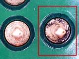
Annular ring de-wetting could be caused by a number of things. There could be contamination in the holes left over from the circuit board manufacturing process. The most likely culprits are solder mask residues, legend marking inks and the like which are designed to cause de-wetting of solder. Solder mask is typically applied before ENIG so solder mask residues would cause a defect in the ENIG plating as well. ENIG defects (missing ENIG) should be visible through inspection of the plated holes. If the annular ring de-wetting is a fairly small area then it may be difficult to find defects in the ENIG plating without cross sectioning. Legend marking ink is often applied after ENIG plating and is typically applied through screen printing. There is a possibility of ink bleeding into the holes when screen printing, especially if the marking ink is placed close to the holes. Once cured it is very difficult to remove and it will resist soldering. Legend marking ink can be more difficult to see in the ENIG plated holes because the color may be similar to the gold finish, especially if white ink is used. There is also a possibility of other types of residues from the circuit board process. Annular ring shaped residues could come from any water rinsing process used after ENIG plating, especially if the water is contaminated with process chemistry. Water tends to form a meniscus in holes and can dry in that form leaving behind a ring shaped deposit. Annular ring shaped de-wetting can also be caused by localized heat sinking if a heavy copper inner layer is connected to the hole. The connection point of the heavy copper inner layer is essentially a cool spot in the hole which will not be wetted with solder properly unless it reaches soldering temperature. In selective soldering, this can be difficult with high thermal mass circuit boards. The heat for soldering is transferred through the solder flowing from the selective nozzle which is relatively small as compared to a wave soldering system. This leads to longer contact times and higher soldering temperatures for selective soldering systems. Once the ENIG gold layer is dissolved into the solder, then the solder must wet the nickel layer. If the contact times are excessively long, which is often the case with high thermal mass boards, then the nickel can begin to oxidize during soldering. Once nickel oxidizes it is very difficult to wet with solder. This would likely appear as more broad scale de-wetting. I recommend cross sectioning of the holes in question before and after soldering in order to determine what is going on. Failure analysis labs can also assist with analysis of any potential contaminates left in the holes which can lead to the root cause of the issue.
Field Applications FCT Assembly Tony has worked in the electronics industry since 1994. He worked as a process engineer at a circuit board manufacturer for 5 years. Since 1999, Tony has worked for FCT Companies as a laboratory manager, facility manager, and most recently a field application engineer. He has extensive experience doing research and development, quality control, and technical service with products used to manufacture and assemble printed circuit boards. He holds B.S. and M.B.S. degrees in Chemistry.
Dewetting is usually a case where the solder initially wets the surface then pulls back when the surface that was initially wetted becomes liquidus. The cause could be the surface finish not properly bonded to the material below, in your case the gold is not bonded to the nickel base, or there is a wetting issue with the nickel. I would say the first place to check is the bare PCB. I would also carefully check the rest of the board, not just annular rings. A solderability issue could affect all of the solder joints. Since you are seeing the issue at wave and (I assume) not at reflow it may be that the wetting is marginal and the shorter duration above liquids in wave vs reflow is causing the issue at the annular rings. Since reflow is usually above liquidus 60-90 seconds it may have more time to wet a marginal surface. IPC TM-650 will give you some options for testing solderability of bare boards before the assembly process.
PCBA Engineering Liaison General Atomics Electromagnetic Systems Group Kevin has over 30 years of experience in process and manufacturing engineering serving in both EMS and OEM companies. Expertise includes all aspects of SMT as well as wave solder and CCA materials such as PCBs, solder material, and component finishes. Kevin has developed processes for thousands of assemblies from stencil printing to conformal coating and testing.
The selective annular ring de-wetting (SAD) phenomenon occurs during Pb-wave soldering assembly and significantly affects the contact side of the annular ring. De-wetting can arise due to black pad phenomena where mud crack appears on the PCB surface. This appearance results from the consumption and corrosion of nickel during the immersion gold plating process. A scanning electron microscope (SEM) analysis is performed on the cross-sections of the bare PCB pads to discover the failure before the PCBA assembly process.
Director of Sales and Marketing Sierra Circuits Amit Bahl started to work at Sierra Circuits in 2006 where he formed strong relationships with his customers working with them on flex PCBs, HDI, controlled impedance, etc. In 2009, he was promoted Director of Sales and Marketing.
|
|||||||
| Submit A Comment | |||||||
|
Comments are reviewed prior to posting. You must include your full name to have your comments posted. We will not post your email address. |


|
Free Newsletter Subscription
Circuitnet is built for professionals who bear the responsibility of looking ahead, imagining the future, and preparing for it. Insert Your Email Address |
|
|