|

|
|

| Ask the Experts | |||||||
|
|||||||
|
August 9, 2024 - Updated January 11, 2017 - Originally Posted Solder Balling Splash After Reflow
Details:
B.G. |
|||||||
| Expert Panel Responses | |||||||
|
Although sometimes related to oxidized paste or paste that sat on the PCB too long before reflow, solder balls are very often reflow profile related. In general, this can be attributed to too slow or too fast of a reflow ramp rate. Heating up an assembly too quickly will not allow the volatiles in the paste to be driven off before paste becomes molten. A combination of volatiles and molten solder will result in solder spatter (balls) and flux spatter. Check the ramp rate in the first 90 seconds of the profile. Run recommended profile and see if the problem persists.
Senior Applications Manager AIM Solder Mr. Pigeon has been Senior Applications Manager with AIM Solder for more than 14 years, assisting customers with SMT Printing, Placement, Reflow, Troubleshooting, and Optimization as well as thorough knowledge of wave and hand solder applications. A combined 30+ years of electronics experience in both OEM and CM Manufacturing.
In my experience solder balls are always hypoeutectic. This means the solder was overheated not underheated. Additional heating will not help dissolve them. Process changes and DOE experiments are required.
President, Consultant Process Solutions Consulting Inc. Lee Levine has been a Process Engineer and Metallurgist in the semiconductor industry for 30 years. He now operates his own company Process Solutions Consulting Inc where he consults on process issues and provides SEM/EDS and metallography services.
Some solder pastes are prone to leaving solder balls under SMD components. This depends largely upon the amount of solder paste printed and the design of the stencil apertures. Solder balling under SMD components can be dramatically reduced through the use of home plate or "U" shaped apertures. The idea is to remove some of the solder paste from the inside edges of the pads to limit the amount of solder paste that can flow under the component during reflow. This doesn't necessarily help to solve the root cause of the issue, but it can help to eliminate the symptoms. The circuit boards themselves might have an effect on this solder balling issue. The HAL finish will vary in volume of solder quite a bit from pad to pad, and board supplier to supplier. That could affect the overall volume of solder in the joints. Higher solder volumes will tend to lead to more solder balling. The surface texture of the solder mask also plays a role. Matte finish solder masks tend to resist or repel solder balls more effectively than glossy solder masks. A semi-matte mask from one supplier might not perform the same as a semi-matte mask from another supplier. The board manufacturers might be using different brands or textures of solder mask and therefore could show differences in solder balling. The Galden solvent used in vapor phase reflow tends to spread the flux residue farther than it would normally spread in convection reflow. This might lead to solder balls traveling with the flux farther under the SMD components. In some cases the amount of flux used in the solder paste can be reduced for use in vapor phase reflow. This would help limit the spread of the solder paste flux. I recommend that you speak with your solder paste supplier for specific solder paste and profile recommendations for use with vapor phase reflow.
Field Applications FCT Assembly Tony has worked in the electronics industry since 1994. He worked as a process engineer at a circuit board manufacturer for 5 years. Since 1999, Tony has worked for FCT Companies as a laboratory manager, facility manager, and most recently a field application engineer. He has extensive experience doing research and development, quality control, and technical service with products used to manufacture and assemble printed circuit boards. He holds B.S. and M.B.S. degrees in Chemistry.
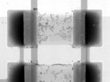
The small, uniform size of most of the balls visible on the x-ray image strongly suggests to me that they are individual solder paste spheres that have not coalesced. If this is the case, then they must be getting separated from the main paste deposit by some mechanism. The observed dependency on the PWB supplier should be a major clue. Some possible mechanisms are: 1.
The inherent rapid heating of the vapor phase process, along with the solvency of the perfluorinated liquid on the flux vehicle, may well be playing a significant part. A process-centric solution would be preferred to trying to control the geometry of the space under the component, which might prove difficult and/or expensive. Some things to consider:
Process Engineer Astronautics Fritz's career in electronics manufacturing has included diverse engineering roles including PWB fabrication, thick film print & fire, SMT and wave/selective solder process engineering, and electronics materials development and marketing. Fritz's educational background is in mechanical engineering with an emphasis on materials science. Design of Experiments (DoE) techniques have been an area of independent study. Fritz has published over a dozen papers at various industry conferences.
Your "Solder Balling Splash After Reflow" description and associated pictures are a good start. But unfortunately, I need more information to isolate root cause/s . Hence my response below may appear vague. Here are a few places to start looking until you can provide more information:
Fellow Raytheon Mark has over 35 years of experience in electronics fabrication, quality, and reliability while working for Raytheon RMD, IEC Electronics, GE, Motorola, ORS, etc. He has most recently taken the role as a Fellow at Raytheon in Tucson, AZ; prior to that, he established IEC Electronics Analysis and Testing Laboratories (IATL), LLC in Albuquerque, NM, for electronics and material analysis testing in the military, medical, and industrial industries. His expertise includes PCB, PCBA, components, and analytical and electrical analysis techniques.
By reading the details of the question I believed you've solved your issue. If you experience solder ball with only one vendor I'd recommend you inspect the bare PCB's before they hit the production floor. There is a possibility that your board vendor might not have its HASL process under control thus generating the solder balls. By the picture you sent I see a lot of solder balls lodged inside the pad area and you can also see a major blow hole in that pad exposing the trace that connect to the other component. It all points toward the vendor.
Senior Manufacturing Engineer Northrop Grumman Edithel is a chemical engineer with 20 year experience in manufacturing & process development for electronic contract manufacturers in US as well as some major OEM's. Involved in SMT, Reflow, Wave and other assembly operations entailing conformal coating and robotics.
From your problem statement, I do not know if you have the same PCB from different suppliers and have problem with one of the supplied board. I have seen a similar problem with a board that had glossy finish - it was the only one that we've had solder balling issues with - all the other ones (matte finish) were fine. The solder mask can have an important impact on the quality of the reflow process. Other than this, assure that:
Engineering and Operations Management Independent Consultant Georgian Simion is an independent consultant with 20+ years in electronics manufacturing engineering and operations.
Contact me at georgiansimion@yahoo.com. |
|||||||
| Submit A Comment | |||||||
|
Comments are reviewed prior to posting. You must include your full name to have your comments posted. We will not post your email address. |


|
Free Newsletter Subscription
Circuitnet is built for professionals who bear the responsibility of looking ahead, imagining the future, and preparing for it. Insert Your Email Address |
|


|