|


|
|

| Ask the Experts | |||||||
|
|||||||
|
March 9, 2026 - Updated February 25, 2026 - Originally Posted BGA Solder Ball Wetting
P.O. |
|||||||
| Expert Panel Responses | |||||||
|
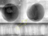
It is clear from the X-ray image that the solder balls have not been deformed/reflowed and thus not wetted to their lands/pads. An obvious defect is a defect regardless of how one may interpretate the wording of the standard. If the wording is not clear, the GEA/IPC welcomes new standards writing committee members who are willing to use their “technical expertise to improve IPC standards” at [https://www.electronics.org/join-committee-home-page].
Senior Project Engineer Electronic Controls Design Inc Paul has been with Electronic Controls Design Inc. (ECD) in Milwaukie, Oregon for over 45 years as a Senior Project Engineer. He has seen and worked with the electronic manufacturing industry from many points of view, including: technician, engineer, manufacture, and customer. His focus has been the design and application of measurement tools used to improve manufacturing thermal processes as well as moisture sensitive component storage solutions.
After reviewing the provided X-ray image, we would like to clarify and further elaborate on the interpretation regarding the alleged “incomplete wetting to land” condition under IPC-A-610J, 8.3.12.3 (Surface Mount Area Array – Solder Connections). Specifically, it is important to distinguish between geometric solder coverage and true metallurgical wetting. In BGA assemblies, the final solder ball footprint after reflow is governed by surface tension equilibrium and solder volume, and it is not required by IPC-A-610J to achieve full circumferential pad coverage. Apparent reduced spread or asymmetry observed in X-ray imaging does not, by itself, constitute evidence of incomplete wetting. “Incomplete wetting,” in the IPC technical sense, refers to the absence of a continuous metallurgical bond between the solder and the base metal surface. This condition cannot be conclusively determined through radiographic imaging alone and requires cross-sectional analysis to confirm interfacial integrity and proper intermetallic compound (IMC) formation. Recommended follow-up evaluation (to confirm wetting at the solder-to-land interface):
Should further analytical confirmation be required, AMMSA Solutions has the capability to perform the above evaluations, including multi-angle and 3D X-ray analysis, precision microsectioning, metallographic evaluation of IMC formation, and mechanical integrity testing. We would be pleased to support a detailed failure analysis to objectively determine compliance with IPC-A-610J criteria.
Engineering Director / Master IPC Trainer (MIT) AMMSA Solutions More than 20 years of technical experience in the electronics industry in roles ranging from Process & Project Engineer to engineering manager and Technical Applications Engineer for Latin Americas. IPC Master Trainer, International speaker and consultant.
There is a yellow arrow pointing to the right solder ball, so I am assuming that is the only issue you are talking about. The left solder ball appears normal. The right solder ball the arrow is pointing to DOES show non-wetting out to the edge of the board pad, from about 270 degrees to almost 360 degrees, and as such it is not at all completely round. There are 2 things can be said about this image, and 4 possible causes that come to mind: 1. It DID in fact go into reflow.It may not be complete reflow, however. 2. It DID NOT completely wet over the entire board pad. This may have been caused by either insufficient dwell (time above solidus) or it may be due to the pad's inability to completely wet to the molten solder, either from a final finish issue or solder mask encroaching up onto the pad edge, or insufficient heat. As to whether this is a defect condition, it is impossible to tell. But it most definitely is at least a PROCESS INDICATOR, and as the experts have noted, further investigation is required using oblique-angle X-ray or 3D lateral X-ray to provide more information. If it is the only solder ball with this condition on multiple PWBs of the same P/N, I would treat it as a one-off, document it, and rework it with a simple reflow where tacky flux is applied around the perimeter of the part, the board is heated to liquify the tacky flux and the liquid flux is blown under the BGA thoroughly from all 4 sides, and then the BGA is brought up to reflow temperatures, cleaned, and X-rayed again. If it passes, good. If it doesn't, it should be removed to determine the cause of the non-wetting. On the other hand, if there are several of these defects seen but only on some boards and not others, and there is no indication that they are tied to a single fabrication lot or date code, then I would look at the reflow profile and make sure it is hot enough that it can overcome the oven loading during production, when there may be many boards in the oven at a time rather than just one board that was used to set up the profile. Oven loading is a phenomena not understood or often overlooked by engineers and technicians. A single board going through the oven sees a much hotter profile than 4, 5, or more boards going through at once; the oven's inability to recover in between each board can cause borderline low reflow temps, leading to insufficient time in liquidus or insufficient time for the board itself to get hot enough for the molten solder to flow and wet properly. Remember: molten solder flows where there is sufficient heat for it to do so.
Advanced Engineer/Scientist General Dynamics Richard D. Stadem is an advanced engineer/scientist for General Dynamics and is also a consulting engineer for other companies. He has 38 years of engineering experience having worked for Honeywell, ADC, Pemstar (now Benchmark), Analog Technologies, and General Dynamics.
|
|||||||
| Submit A Comment | |||||||
|
Comments are reviewed prior to posting. You must include your full name to have your comments posted. We will not post your email address. |


|
Free Newsletter Subscription
Circuitnet is built for professionals who bear the responsibility of looking ahead, imagining the future, and preparing for it. Insert Your Email Address |
|


|