|


|
|

| Ask the Experts | |||||||
|
|||||||
|
July 29, 2025 - Updated July 18, 2018 - Originally Posted IPC SOIC Defect Question
Reference: IPC-A-610, section 8.3.5.5 Flat Gull Wing Leads D.O. |
|||||||
| Expert Panel Responses | |||||||
|
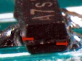
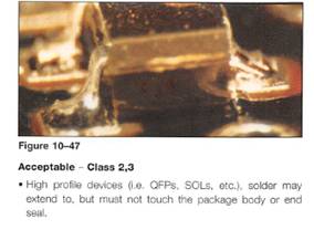
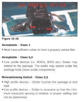
This condition originated with the large pads and small short leads as it was called in the beginning, circa 1980-90s. The physical leads were coming off from the bottom half of the component thickness. In Revision B of 610, this condition was identified as Low Profile Components (SOT and SOICs), the components with leads coming off the upper half of the component (QFPs and SOLs) were called High Profile Components as shown in the attached pictures. With the amount of solder which was deposited on the pads with 6 and 8 mil stencils which were used and typical at the time and such small leads on SOT and SOIC the solder would climb to the top of the lead and contact the component body. The only way these component could be used at the time was to allow this condition to exist. The following was Adapted from IPC-A-610 Rev B Section 10 Page 119
This was also the criteria in Rev C circa 2000. In Rev D onward the committee rephrased the criteria to include the word Plastic Component in the definition and it has been that way ever since. The other issue was the plating on the leads was tin/lead which allowed the solder to flow up the leads rather easily. There were no issues with the moisture entrapment with these component as they were not hermetically sealed, hence no problems were experienced with this condition. The only components which had lead seal issues were the ceramic components and this condition was not allowed on ceramic components. I hope this explains the condition and if more is needed please don't hesitate to contact me at your convenience.
Vice President, Technical Director EPTAC Corporation At EPTAC Corporation, Mr. Lambert oversees content of course offerings, IPC Certification programs and provides customers with expert consultation in electronics manufacturing, including RoHS/WEEE and lead free issues. Leo is also the IPC General Chairman for the Assembly/Joining Process Committee.
When solder touches a ceramic or metal component's body it could break the seal between the lead and the body allowing solder to sip through shorting out the component or allowing moisture to get in. In the case of a plastic body it allows this to happen only for Class I since it is consumer electronics. I read that IPC did not have enough data to categorize it as a defect for Class 1, 2 & 3.
Senior Manufacturing Engineer Northrop Grumman Edithel is a chemical engineer with 20 year experience in manufacturing & process development for electronic contract manufacturers in US as well as some major OEM's. Involved in SMT, Reflow, Wave and other assembly operations entailing conformal coating and robotics.
Historically the reason for this difference is that the ceramic or glass-bodied parts have glass seals that may be damaged by the mechanical forces and/or thermal shock of direct contact with molten solder. In wave or hand soldering applications, this is certainly a concern, but in reflow, less so. There is still the issue of increased mechanical stresses at the point where the lead exists the body, however, and if you have that much solder there are design and/or process issues that need to be addressed if possible.
Process Engineer Astronautics Fritz's career in electronics manufacturing has included diverse engineering roles including PWB fabrication, thick film print & fire, SMT and wave/selective solder process engineering, and electronics materials development and marketing. Fritz's educational background is in mechanical engineering with an emphasis on materials science. Design of Experiments (DoE) techniques have been an area of independent study. Fritz has published over a dozen papers at various industry conferences.
Ceramic components such as ceramic quad flat pack (CQFP) or other similar ceramic devices have a very low CTE (coefficient of thermal expansion) die material and are in most cases hermetically sealed to low-CTE lead-frame material such as Alloy 42 or Kovar. Direct contact with molten solder or excessive rework cycles can result in a cohesive fracture or intermittent open interconnections between the die material and the lead-frame. In some cases these types of failures can only be detected after highly accelerated life test (HALT) or highly accelerated stress screen (HASS) testing.
General Manager Nordson SELECT Carlos Bouras is the General Manager of Nordson SELECT and has over 30 years of experience in the electronics manufacturing industry. Carlos's expertise is in process engineering, product development and manufacturing operations. For the past 15 years Carlos has focused specifically on automated assembly issues and is the holder of several US patents for non-contact dispensing and precision dispensing of adhesives for the packaging of microprocessor devices.
The issue with "IPC SOIC Defect" relative to if solder touches the body of a Metal, Ceramic, or Plastic component :
Fellow Raytheon Mark has over 35 years of experience in electronics fabrication, quality, and reliability while working for Raytheon RMD, IEC Electronics, GE, Motorola, ORS, etc. He has most recently taken the role as a Fellow at Raytheon in Tucson, AZ; prior to that, he established IEC Electronics Analysis and Testing Laboratories (IATL), LLC in Albuquerque, NM, for electronics and material analysis testing in the military, medical, and industrial industries. His expertise includes PCB, PCBA, components, and analytical and electrical analysis techniques.
|
|||||||
| Submit A Comment | |||||||
|
Comments are reviewed prior to posting. You must include your full name to have your comments posted. We will not post your email address. |


|
Free Newsletter Subscription
Circuitnet is built for professionals who bear the responsibility of looking ahead, imagining the future, and preparing for it. Insert Your Email Address |
|


|