|


|
|

| Ask the Experts | |||||||
|
|||||||
|
February 5, 2026 - Updated January 24, 2017 - Originally Posted Solder Balling Prediction FormulaWe have experienced mid chip solder balling on some passives. Is there a mathematical calculation that can be used to predict solder balling for a give package size? Ideally we would like to design our stencil apertures to ensure no mid chip solder balls. Is there a mathematical way to help with this problem? R.W. |
|||||||
| Expert Panel Responses | |||||||
|
I don't believe there is a mathematical way to solve for this type of defect but here are some ideas to minimize or completely remove the mid-chip solder ball by modifying your stencil:
Senior Manufacturing Engineer Northrop Grumman Edithel is a chemical engineer with 20 year experience in manufacturing & process development for electronic contract manufacturers in US as well as some major OEM's. Involved in SMT, Reflow, Wave and other assembly operations entailing conformal coating and robotics.
I am not aware of a mathematical formula to predict mid-chip beading on passive components. The stencil design can be changed to minimize this issue. Typically a "U" shape or inverted "home plate" shape can help. The idea is to remove solder paste from under the body of the component which limits the potential of spread of solder. Most stencil suppliers can give more specific recommendations.
Field Applications FCT Assembly Tony has worked in the electronics industry since 1994. He worked as a process engineer at a circuit board manufacturer for 5 years. Since 1999, Tony has worked for FCT Companies as a laboratory manager, facility manager, and most recently a field application engineer. He has extensive experience doing research and development, quality control, and technical service with products used to manufacture and assemble printed circuit boards. He holds B.S. and M.B.S. degrees in Chemistry.
Many variables will contribute to solder balling. The solder paste should be the right type for aperture size. Make sure the paste is fresh and not drying out. The stencil should be cut to the component manufactures recommendations. The printing process needs to be robust applying the proper solder paste volume for the components in question. This can be confirmed using an automated solder paste inspection process (SPI). Some screen printer have this build in. The printing process may require more frequent under screen cleaning to avoid depositing solder paste on the board mask. If there are no problems found with the printing process, you will need to review your reflow profile. Different paste require different soak times.
Manufacturing Applications Specialist Cirtronics Corp. Mr. Bush has over 30 years of experience in electronics contract manufacturing. Major areas of expertise include through-hole, SMT, wave, and selective soldering.
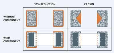
The mid-chip solder ball occurs when solder is squeezed under the component and away from the pad and is unable to coalesce back during reflow, remaining hidden under the component or appearing out to the side of the device. Several causes for mid-chip solder balling have been suggested and include excess solder paste on the pad, poor hot slump and insufficient wetting. The mid-chip solder ball phenomenon tends to occur more frequently with chip resistors due to the fact that they have tinning on three sides and a reduced solderable surface as compared to capacitors, though capacitors may also be subject to this defect. The reported occurrences of mid-chip solder balls have changed as the industry has moved toward more miniaturized components and lead-free solder paste materials.
The results of this part of the study revealed that reducing slump either by adding a gelling agent or increasing the metal content in the solder paste did lower the occurrence of mid-chip solder balling, but it was not the only factor; reduction of the stencil's inner aperture wall also played an important - if not more significant -- role. While paste characteristics are important, reducing aperture area through the use of "u" or "crown" shaped designs has the greatest effect on mid-chip solder balling reduction.
Marketing 360-Biz Douglass Dixon is the Chief Marketing Officer for 360 BC Group, a marketing agency with offices throughout the US. 360 BC specializes in consulting and implementing successful marketing programs that utilize the latest in marketing, sales and technology strategies. As an electronics veteran, Dixon has worked in the industry for over 30 years for companies like Henkel, Universal Instruments, Camelot Systems, and Raytheon. Dixon's electronics industry experience includes a broad skill set that includes engineering, field service, applications, product management and marketing communications expertise.
Solder balling is a process problem that can occur from multiple causes. Stencil aperture design and stencil thickness are just 2 of them. I do not think that you can mathematically predict solder balling but getting the stencil aperture and thickness as recommended per package size and design is one way to avoid it. Next, ensure that:
Engineering and Operations Management Independent Consultant Georgian Simion is an independent consultant with 20+ years in electronics manufacturing engineering and operations.
Contact me at georgiansimion@yahoo.com. Mid Chip Solder Beading is a problem caused by a few Technical issues and the main cause is when the PCB and Stencil are not perfectly gasketed together leaving a tiny gap for the paste to creep under, build up on the underside of the stencil and produce a bead. This can also be seen when automatic height pins for board support don't fire properly given a gap for the paste to creep under. You can also exaggerate this problem if you over pressurize the squeegees and squeeze the flux(shear)thin and again force the paste in the gap left. Or simply and most commonly already print slightly off pad with improper wells around the pad to enable pull back and there's your solder bead.
Technical Sales Manager BLT Circuit Services Ltd Greg York has over thirty two years of service in Electronics industry. York has installed over 600 Lead Free Lines in Europe with Solder and flux systems as well as Technical Support on SMT lines and trouble shooting.
|
|||||||
| Submit A Comment | |||||||
|
Comments are reviewed prior to posting. You must include your full name to have your comments posted. We will not post your email address. |


|
Free Newsletter Subscription
Circuitnet is built for professionals who bear the responsibility of looking ahead, imagining the future, and preparing for it. Insert Your Email Address |
|


|