|


|
|

| Ask the Experts | |||||||
|
|||||||
|
October 28, 2025 - Updated October 19, 2016 - Originally Posted Recommended Fiducial Shape
J.M. |
|||||||
| Expert Panel Responses | |||||||
|
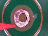
This defect is not the result of the fiducial shape. All fiducial designs work fine with a normal HASL process. This looks like a touch mark prior to solder solidification.
President S T and S Testing and Analysis Gerald O'Brien is Chairman of ANSI J-STD 003, and Co Chairman of IPC 4-14 Surface Finish Plating Committee. He is a key member of ANSI J-STD 002 and 311 G Committees Expert in Surface finish, Solderability issues and Failure analysis in the PWA, PWB and component fields.
What type of equipment is rejecting this as a fiducial? Possibly a plus symbol (+) would work if your equipment will accept.
Director of Corporate Quality Assurance Delta Group Electronics Inc. Tod has been working in the Aerospace Electronics Industry for 25 years, beginning with 4+ years working for PCB fabricator ending as the Quality Manager and 20 years with Delta Group Electronics Inc. an AS9100 registered electronics contract manufacture. Currently position is Director of Corporate Quality Assurance.
The IPC SMEMA design standard for fiducial marks is a solid filled circle. Ge the standard from IPC.
North America Sales Manager Essegi Automation Mr. Black was the President and Co-Founder of Zevatech in 1977 and introduced first Pick and Place System at Nepcon West 1980. Bob is now the President, CEO and Co-Founder of Juki Automation Systems. He is also a Co-Founder of the SMEMA Council of IPC. He serves as a member of SMTA and SEMI..
I recommend using a full circle instead of the donut.
Senior Manufacturing Engineer Northrop Grumman Edithel is a chemical engineer with 20 year experience in manufacturing & process development for electronic contract manufacturers in US as well as some major OEM's. Involved in SMT, Reflow, Wave and other assembly operations entailing conformal coating and robotics.
In making some assumptions about your board design.... we can only speculate from this photo/question. The PCB should not be "pooling" solder on the fiducial (or anywhere), this is a PCB house related issue and usually occurs with low cost pattern plating. That said, your board should be checked for cleanliness and if it's more than a Class 2 board this could be a long term problem for the product. In most PCBA Designs, I would allow LPI solder mask over the fiducial mark. Our camera's were capable of seeing the image with Soldermask over the top of the fiducial. Soldermask is less reflective, and would ensure my camera lighting etc was more robust. You may try masking over fiducial mark, to avoid variation of HASL on the pad. They call it HASL for a reason.
Capital Equipment Operations Manager Specialty Coating Systems Rodney is currently Operations manager at SCS coatings, Global Leader in Parylene and Liquid Coating equipment. Rodney applies his BS in Computer Integrated Manufacturing from Purdue University, along with 20+ years of Electronic manufacturing and Equipment Assembly, to direct the Equipment business at SCS Coatings. "We provide unique, value added coating equipment solutions for our customers". Including conformal, spin and Parylene coating expertise.
The HASL process tends to create thicker "bumps" of solder on small pads and thinner more flat deposits on large pads. Decreasing the copper area of the fiducials from a circle to a donut might have aggravated the issue, creating larger bumps. We suggest increasing the size / copper area of the fiducials if possible. Then the HASL process might be able to blow the solder a little more flat in that area.
Field Applications FCT Assembly Tony has worked in the electronics industry since 1994. He worked as a process engineer at a circuit board manufacturer for 5 years. Since 1999, Tony has worked for FCT Companies as a laboratory manager, facility manager, and most recently a field application engineer. He has extensive experience doing research and development, quality control, and technical service with products used to manufacture and assemble printed circuit boards. He holds B.S. and M.B.S. degrees in Chemistry.
|
|||||||
| Submit A Comment | |||||||
|
Comments are reviewed prior to posting. You must include your full name to have your comments posted. We will not post your email address. |


|
Free Newsletter Subscription
Circuitnet is built for professionals who bear the responsibility of looking ahead, imagining the future, and preparing for it. Insert Your Email Address |
|


|