|


|
|
| Ask the Experts | |||||||
|
|||||||
|
March 9, 2026 - Updated February 25, 2026 - Originally Posted BGA Solder Ball Wetting
P.O. |
|||||||
| Expert Panel Responses | |||||||
|
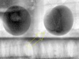
It is clear from the X-ray image that the solder balls have not been deformed/reflowed and thus not wetted to their lands/pads. An obvious defect is a defect regardless of how one may interpretate the wording of the standard. If the wording is not clear, the GEA/IPC welcomes new standards writing committee members who are willing to use their “technical expertise to improve IPC standards” at [https://www.electronics.org/join-committee-home-page].
Senior Project Engineer Electronic Controls Design Inc Paul been with Electronic Controls Design Inc. (ECD) in Milwaukie, Oregon for over 39 years as a Senior Project Engineer. He has seen and worked with the electronic manufacturing industry from many points of view, including: technician, engineer, manufacture, and customer. His focus has been the design and application of measurement tools used to improve manufacturing thermal processes and well as moisture sensitive component storage solutions.
After reviewing the provided X-ray image, we would like to clarify and further elaborate on the interpretation regarding the alleged “incomplete wetting to land” condition under IPC-A-610J, 8.3.12.3 (Surface Mount Area Array – Solder Connections). Specifically, it is important to distinguish between geometric solder coverage and true metallurgical wetting. In BGA assemblies, the final solder ball footprint after reflow is governed by surface tension equilibrium and solder volume, and it is not required by IPC-A-610J to achieve full circumferential pad coverage. Apparent reduced spread or asymmetry observed in X-ray imaging does not, by itself, constitute evidence of incomplete wetting. “Incomplete wetting,” in the IPC technical sense, refers to the absence of a continuous metallurgical bond between the solder and the base metal surface. This condition cannot be conclusively determined through radiographic imaging alone and requires cross-sectional analysis to confirm interfacial integrity and proper intermetallic compound (IMC) formation. Recommended follow-up evaluation (to confirm wetting at the solder-to-land interface):
Should further analytical confirmation be required, AMMSA Solutions has the capability to perform the above evaluations, including multi-angle and 3D X-ray analysis, precision microsectioning, metallographic evaluation of IMC formation, and mechanical integrity testing. We would be pleased to support a detailed failure analysis to objectively determine compliance with IPC-A-610J criteria.
Engineering Director / Master IPC Trainer (MIT) AMMSA Solutions More than 20 years of technical experience in the electronics industry in roles ranging from Process & Project Engineer to engineering manager and Technical Applications Engineer for Latin Americas. IPC Master Trainer, International speaker and consultant.
|
|||||||
| Submit A Comment | |||||||
|
Comments are reviewed prior to posting. You must include your full name to have your comments posted. We will not post your email address. |


|
Free Newsletter Subscription
Circuitnet is built for professionals who bear the responsibility of looking ahead, imagining the future, and preparing for it. Insert Your Email Address |
|


|