|
|
|
|
|
|
|
|
|
|
|
|
| Ask the Experts | |||||||
|
|||||||
|
April 2, 2024 - Updated February 9, 2016 - Originally Posted Partially Visible or Hidden Solder Connections
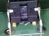
The issue primarily arises out of the 75% barrel fill clause in IPC-A-610 - in which the QE group believes that, if the only view you have from a manual inspection standpoint is not of a top-down view, you have to assume the part is good. The photo shows a component on a PCBA that we build and inspect. The QE is arguing that the angle of view is inadequate to make a quality call that the barrel fill is not sufficient. I don't feel that this is how this portion of the standard is to be read. Being a CM, it is not necessarily feasible to add an X-Ray inspection to the process due to added cost. I would like to know how others in the industry work around situations like this? M.S. |
|||||||
| Expert Panel Responses | |||||||
|
A summary of section 4.18.3 in J-STD-001 states:
Field Applications FCT Assembly Tony has worked in the electronics industry since 1994. He worked as a process engineer at a circuit board manufacturer for 5 years. Since 1999, Tony has worked for FCT Companies as a laboratory manager, facility manager, and most recently a field application engineer. He has extensive experience doing research and development, quality control, and technical service with products used to manufacture and assemble printed circuit boards. He holds B.S. and M.B.S. degrees in Chemistry.
For nearly all PTH components, there is usually some clearance between the bottom of the part and the surface of the PWB for cleaning purposes, but not always. Sometimes you can use inspection prisms along with a good microscope to at least be able to see evidence of wetting under the part. Inspection prisms are different than mirrors in that they go flush to the PWB surface, allowing you to see even under very tight gaps. If there is no way to see just how much hole-fill is achieved visibly, you then have three choices: 1) You can complete the assemblies except for conformal coating and use X-ray to validate the hole-fill, or you can arrange with a local non-destructive testing company that provides X-ray inspection. They can do the X-ray and email you the images, identified by PN and SERNO and REFDES number, so you know which require rework. Just Google up "non-destructive testing, X-ray" for a list of companies who you can arrange this with. But be warned, it is not cheap. If it is absolutely imperative (extremely high reliability product) where absolute proof of hole fill on 100% of the product is required, then it is also possible to use the X-ray service house to perform 100% X-ray of all of the product and email you the X-ray images and ship back any CCAs you deem to be unsatisfactory. The X-ray images can be used as the process verification and you can arrange to send them to your customer as well. For short-term contracts it is possible to lease an X-ray machine, and this is often a very cost-effective solution. Just make sure your floor (even if concrete at ground level) is capable of handling the weight of an X-ray machine; the smallest ones can weigh 3500 lbs, the larger easily go over 8000 lbs. That's four tons, baby. 2) Or you can use a temporary spacer, preferably a thin shim of .010" thick FR-4 (or thicker, if no fit limit exists) or use a water-soluble spacer to hold the part up off the board during the soldering operation (AABUS). If your component height limit, your use environment, or your customer does not allow that, then 3) You can qualify your process by implication. If this is the case, the soldering process must be automated. Manual soldering cannot be qualified by implication. Ok, in your case you cannot afford to buy an expensive X-ray machine in order to perform option 1, and your customer does not want to lift the part up off the board even just .010" to allow prism inspection, or the height limit precludes it. The outside X-ray option can be expensive. What then? You can take a scrap CCA (or two or three), place some of the "uninspectable" components onto the scrap board(s), and duplicate your exact production set-up for the automated soldering process, whether it is selective solder or wave solder. You document all of the operating parameters, the solder temperature, the flow rate, the flux level, the conveyor speed or the nozzle speed and height, the pre-heater profile, everything. When you think you have the optimum process settings, you then solder your scrap CCA(s), wash and clean them, and then microsection through at least a sample of 8 of the "uninspectable" solder joints. If (if and only if) your micro-sections show you achieved 100% hole-fill on all 8 locations, you then fully document this process qualification, and you "lock down" the process settings. Every time a lot of CCAs are run in production thereafter, you have an Inspector review all of the settings prior to running production through the process. To ensure nothing has changed over time, you then repeat the in-house micro-sectioning procedure on a witness sample once a week, or once a month, or once a quarter, or whatever frequency you and your customer feels comfortable with (AABUS), depending on the device's use or function. Your customer must buy in to this, or change the design or the part, or perhaps go in with you on an X-ray system to defray the cost, along with an agreement as to how the X-ray machine is to be dispositioned at the end of the contract. One more tip: I have actually designed in a hole pattern in the breakaway tabs, if there are any, to sacrifice a single component (the same component) that represents the lot of boards run with that machine setup. If the setup changes, a new witness part should be run and either X-rayed again or sectioned. The witness part provides proof, by implication, that the rest of the uninspectable components are getting 100% hole-fill. The sampling rate is AABUS, and is a great cost reducer if you need to go outside for X-rays, or have to perform microsections in-house (or outside). Continually seeing 100% hole fill in the sampled X-rays or witness samples over time will allow both you and your customer to sleep at night (or during the day in the office if you're Management), knowing your product is going out the door with a very, very high probability of meeting the Class 2 or 3 requirements.
Advanced Engineer/Scientist General Dynamics Richard D. Stadem is an advanced engineer/scientist for General Dynamics and is also a consulting engineer for other companies. He has 38 years of engineering experience having worked for Honeywell, ADC, Pemstar (now Benchmark), Analog Technologies, and General Dynamics.
Your process team should conduct a study to ensure that the process in reproducible. If you use data that reflects barell fill greater then 75%, with process variation then why would your QE team need to check for this? Alternately you and use SPC checks over a few months to determine the risk of poor barell fill. Company's which run volume via wave solder make use of a dumpy PTH, which is used by the QE team to check barell fill visually, hence no need for x-ray inspection.
Process Engineering Manager - Electronics Altech UEC, South Africa Currently with Altech UEC and responsible for technology road map in PCBA electronic manufacturing and technical support for PCBA electronic manufacturing for Altech UEC and its JDM's. Over 7 years in SMT, Radial Insertion, Wave solder & Test Applications.
Since one side is covered, I believe that without X-RAY it is almost impossible to conclude that you have 75% hole fill. However there are other options. Assuming that the soldering process is under control, one alternative will be to make a micro-sectional study. The micro-section will show how much hole-fill are you providing and it will also let you know if adjustments to the process need to be made.
Senior Manufacturing Engineer Northrop Grumman Edithel is a chemical engineer with 20 year experience in manufacturing & process development for electronic contract manufacturers in US as well as some major OEM's. Involved in SMT, Reflow, Wave and other assembly operations entailing conformal coating and robotics.
In situations similar to the one you show, it is often possible to get a very good estimate of the depression depth. In some cases where we have a very thick PWB and/or a relatively tight lead-to-hole spacing, it may not be possible. In cases where it is not possible, we cannot assume that "If we can't see that it is defective, it must be good." If I were the customer, I would not accept that. If you cannot inspect it visually, you need to be able to validate hole fill by other means, which could mean x-ray. If I were in the position where I could not implement x-ray due to cost, for the component shown I would tune the process to ensure that I nearly always had 100% fill with a visible topside fillet. That way, I can inspect at an angle, and the very few parts for which I cannot verify 100% fill I can rework. If the rework is limited to a very small number of parts, this will not be a problem. If, however, my process in incapable such that I have even a moderate percentage of parts requiring rework, the cost will spiral out of control.
Process Engineer Astronautics Fritz's career in electronics manufacturing has included diverse engineering roles including PWB fabrication, thick film print & fire, SMT and wave/selective solder process engineering, and electronics materials development and marketing. Fritz's educational background is in mechanical engineering with an emphasis on materials science. Design of Experiments (DoE) techniques have been an area of independent study. Fritz has published over a dozen papers at various industry conferences.
The original intent of this question was to be able to check the bottom side of the solder joint to see whether it met all the requirements of a good solder joint, good wetting to the lead and pad. The other intent was that all the other leads on the component side, which were visible on the printed board were acceptable on both sides of the board. The reasoning behind this was to check the board itself to determine if it was solderable and all the solder has flowed up into the plated through hole that were not tied to any inner layers. If this answer was yes, and the bottom joints looked ok, then the condition was deemed acceptable. Of course today, people can check with X-Ray equipment and make a determination of whether the hole is filled 75% or not, but to my knowledge they may find those conditions, less than 75% hole fill or less than 50% hole fill if tied to an inner layer, but no electrical failure were detected. The industry may not like it when it is view with x-ray, but it is still a good joint and has been for over 50 years. If electrical failures have occurred it is up to them to show proof of failure due to the condition.
Vice President, Technical Director EPTAC Corporation At EPTAC Corporation, Mr. Lambert oversees content of course offerings, IPC Certification programs and provides customers with expert consultation in electronics manufacturing, including RoHS/WEEE and lead free issues. Leo is also the IPC General Chairman for the Assembly/Joining Process Committee.
Reader Comment
I don't know of any part of J-STD or 610 that says you don't have a visible solder connection-or can't verify vertical fill-if you don't have a "top-down" view. In fact, most of the illustrations in 610 are in oblique view. So the view in your photo seems to provide enough visibility to verify this.
As summarized in an earlier response, section 4.18.3 in J-STD-001 states:
John De Leeuw, TE Subcom
|
|||||||
| Submit A Comment | |||||||
|
Comments are reviewed prior to posting. You must include your full name to have your comments posted. We will not post your email address. |


|
Free Newsletter Subscription
Circuitnet is built for professionals who bear the responsibility of looking ahead, imagining the future, and preparing for it. Insert Your Email Address |
|
|
|
|
|
|
|
|