|

|
|

| Ask the Experts | |||||||||||
|
|||||||||||
|
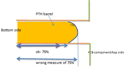
May 12, 2025 - Updated June 19, 2013 - Originally Posted Through Hole Connector Solder Joint Hole FillWhen looking at IPC610D in relation to through hole connectors and Class III level soldering. What is the recommended inspection method to ensure the 75% fill requirement is being met? For many through hole connectors one side is totally covered. R.D. |
|||||||||||
| Expert Panel Responses | |||||||||||
|
When you say that one side is, "totally covered" I'm assuming that you mean that the solder destination side of the component is not visible due to the body of the component. This condition is not addressed in the IPC-A-610D In the case where it is not possible to see one side of the solder joint, you should refer to the J-STD-001E, paragraph 4.18.3. "4.18.3 Partially Visible or Hidden Solder Connections Partially visible or hidden solder connections shall [A1P2D3] meet the following conditions: A. The design does not restrict solder flow to any connection element on the solder destination side lands (e.g., PTH component) of the assembly. B. The visible portion, if any, of the connection on either side of the PTH solder connection (or the visible portion of the SMD connection) is acceptable. C. Process controls are maintained in a manner assuring repeatability of assembly techniques." Essentially, you need to ensure that you don't have hole obstruction, any visible portion of the connection is acceptable, and process controls are in place to ensure that the acceptable condition is repeatable and reliable.
Manager of Assembly Technology IPC Kris Roberson has experience as a machine operator, machine and engineering technician and process engineer for companies including Motorola, and US Robotics. Kris is certified as an Master Instructor in IPC-7711 / 7721, IPC A-610 and IPC J-STD 001.
For class III solder fillet in the past use people to inspect joints using magnifying lights or microscope. Today CM's use AOI program to view solder joints to ensure > 75% fillet is met or better yet exceeding. At some point when the solder profile is fine tuned, they can reduce AOI points.
President and Founder Contract Manufacturing Consultants, Inc. Robert Fried helps leading electronics OEM's develop world-class sourcing strategies for PCBA, cables, precision metals, plastics, modules and complete end-products. Other service areas are supplier risk assessment, comprehensive outsource ...
An x-ray can be used to periodically ensure hole fill. If top side hole fill is used, then there is no concern about hole fill. This would require that the through hole component can be reflow soldered, using solder paste and potentially solder preforms placed in solder paste to ensure adequate volume. Another option which is gaining popularity is the use of low temperature RoHS compliant SnBi solder preforms, flux coated. Replace the wave process with a third reflow process, at 190C peak temperature. The solder washer is sized to ensure 100% hole fill, or more if a fillet is required. Of course, the alloy change needs to be approved by the final customer. Most experts agree that the pull force is not an issue for through hole connectors. And for many classes of electronics, the reliability is sufficient.
Global Product Manager Alpha Mr. Koep is responsible for product planning and technical marketing for the Preform Products at Alpha. He is the co-author of several patents in the areas of soldering applications focusing on reflow and alternative methods.
Our company faces this problem daily since our products (aerospace electronics) use thick PWBs and PTH connectors with high pin counts in multiple rows. The solder destination side of the majority of joints on some of these connectors is difficult or impossible to visually inspect. In these cases, transmission x-ray can almost always provide a method for evaluation of such joints. We have found that even dense, multi-row PTH connectors can be evaluated this way. In order to perform x-ray inspection of such a connector, the component must be viewed off-vertical, at between 30 and 45 degrees. The board must also be rotated so that pins are offset in the image, not directly in front of or behind others. We find that this is almost always feasible. Normally, we set up programs which take the operator to the specific location(s) needed, and set the x-ray parameters for viewing. This should be possible on most full-featured x-ray systems made for electronics work. We use a Phoenix (GE) nanome|x for our work.
Process Engineer Astronautics Fritz's career in electronics manufacturing has included diverse engineering roles including PWB fabrication, thick film print & fire, SMT and wave/selective solder process engineering, and electronics materials development and marketing. Fritz's educational background is in mechanical engineering with an emphasis on materials science. Design of Experiments (DoE) techniques have been an area of independent study. Fritz has published over a dozen papers at various industry conferences.
Some methods that work are X-ray inspection at an oblique angle. Here you can check hole-fill and also if any large voids are present. Larger voids tend to occur more often with lead-free alloys due to the slower wetting behavior. Another is cross-sectioning of a board when the process is fully optimized but this is a destructive method often not preferred. Obviously visual has limitations and more critical builds require confirmation that all sides of a connector are soldered to specification.One side that passes does not mean both sides do.
Senior Market Development Engineer Kester Mr. Biocca was a chemist with many years experience in soldering technologies. He presented around the world in matters relating to process optimization and assembly. He was the author of many technical papers delivered globally. Mr. Biocca was a respected mentor in the electronics industry. He passed away in November, 2014.
There are three methods of verifying PTH hole-fill. The first two are Visual inspection and X-ray. A third method is qualification by implication, where the soldering parameters of an automated solder process are qualified and then validated with a set of microsections using a number of samples. This is considered to be a Gauge Repeatability and Reproducibility (GR&R)method. It cannot be used if the soldering is done by hand, manually, however. Almost all connectors used in the industry have some kind of standoff on the bottom of the connector body to allow for cleaning. While it is true that you may not be able to see under the connector body directly using a microscope because of adjacent components blocking the view, there is almost always enough clearance to use a combination of the microscope and an inspection mirror designed just for that purpose. The ones I like to use are the EMR Mini Mirror Vision Set from Elme: http://www.youtube.com/watch?v=ffJmtV9PC4Y. They also work great for inspection of BGA solder joints. These can be used to verify that the solder flowed through to the top of the CCA. In other words, the solder joint is visible under the component body. This method does not detect large voids inside the barrel, however. The second method is X-ray. This is the best and fastest method. An X-ray can positively identify the full length of the solder joint, and show you how much voiding may be in there. With the third (GR&R) method, even though you cannot validate each and every solder joint directly, you are able to at least show that the automated solder process is a consistent process once qualified and then certified (locked up-no further changes allowed). If this method is used, you can either get a few solder coupons with each lot of PWBs that have the exact same connector hole pattern, and a smaller or similar connector can then be run through the process at the same time that production lots are run (perhaps one solder coupon for every 50 production CCAs run under the same set-up). Then you can periodically micro section the solder coupons, or perhaps you can simply visually verify the topside solder joints on the coupon connector, or use some combination of both methods. The coupon samples should serve as a representative of the lot of CCAs built under that machine setup. If the solder coupon(s) show complete and acceptable hole-fill continuing to be accomplished, then, by implication, you can assume the same is true of the connectors on that lot of production CCAs. There are companies that can perform the micro sectioning for a nominal cost or you can learn to do it yourself (a great skill to have). Micro sectioning methods are covered in IPC-DVD 28 (manual method) and micro-sectional analysis is covered in IPC-DVD30/31. This may be a much cheaper alternative than buying an X-Ray machine if you only need to do this for a single contract. One caveat: if you have a connector with no standoff whatsoever, you will have a gas trap, and no amount of pre-heat or disturbed solder, or jetting, or anything else will provide a complete hole-fill. There has to be a method for the gas (air) to flow out of the topside in order to allow the solder to completely fill the hole and form a good topside fillet. If the connector sits flat over the hole, all bets are off. I would never use any connector without the proper standoff needed for cleaning and inspection purposes.
Advanced Engineer/Scientist General Dynamics Richard D. Stadem is an advanced engineer/scientist for General Dynamics and is also a consulting engineer for other companies. He has 38 years of engineering experience having worked for Honeywell, ADC, Pemstar (now Benchmark), Analog Technologies, and General Dynamics.
This question is interesting from the viewpoint of the requirement of IPC-A-610 and J-STD-001. J-STD-001 states in Section 4.18.3 Partially Visible or Hidden Solder Connections, that the design of the product and the use of the components shall not restrict the flow of solder to any connection element on the solder destination side lands. It also states that the visible portion, if any, of the connection on either side of the PTH solder connection (or the visible portion of the SMD connections is acceptable. And it finally states that process controls are maintained in a manner assuring repeatability of assembly techniques. If the conditions on the board don't meet these requirements then it is a defective condition for Class 3 products. Now, how can one tell if the solder has risen 75% in the pth, is dependent upon how the solder has risen through all the other plated through holes on the board to allow the opportunity to make the assumption that the board is solderable and will solder. Secondly the components have been solderability tested for compliance to the specification. Thirdly there has been some microsections taken to prove the process is in fact capable of producing the required solder joints as required by the specification. Lastly,process controls are in place to maintain the process. If it is imperative that each board and connector be evaluated for 75% hole fill, then X-ray the plated through holes and use that information to satisfy your customer. I hope this somewhat answers the question, as I know the controversy regarding this topic and the positions taken by the various industries. If more information is required please get in touch with me at your convenience.
Vice President, Technical Director EPTAC Corporation At EPTAC Corporation, Mr. Lambert oversees content of course offerings, IPC Certification programs and provides customers with expert consultation in electronics manufacturing, including RoHS/WEEE and lead free issues. Leo is also the IPC General Chairman for the Assembly/Joining Process Committee.
Supplier Quality Leader Ge Healthcare Subrat has 10 year of extensive experience in PCB assembly process optimizing for quality, process includes screen printing, wave, reflow. He has a copyright in stencil design published in Apex Expo2010 at Las Vegas US.
X-Ray inspection works very well for inspecting for voiding and fillet fill.
Vice President Technology Photo Stencil For over 18 years, Dr. Coleman has been the vice president of technology for Photo Stencil, working closely with customers to understand their printing requirements. His efforts have resulted in several new stencil products.
Reader Comment
When we are talking about Class 3 in IPC, we must take as reference of the complete TH module, because hole fill is not the only concern, JSTD001F and IPC A 610F are new revisions.
Master IPC Tariner Luis Alberto Garcia
One other related note on the inspectability subject: Sometimes all it takes to get a minimum of 75% hole fill is to simply pre-tin the connector pins prior to assembly and soldering. Inspection is much easier if you obtain 100% hole fill, and pre-tinning is the best method of improving hole fill.
Advanced Engineer/Scientist General Dynamics Richard D. Stadem is an advanced engineer/scientist for General Dynamics and is also a consulting engineer for other companies. He has 38 years of engineering experience having worked for Honeywell, ADC, Pemstar (now Benchmark), Analog Technologies, and General Dynamics.
|
|||||||||||
| Submit A Comment | |||||||||||
|
Comments are reviewed prior to posting. You must include your full name to have your comments posted. We will not post your email address. |


|
Free Newsletter Subscription
Circuitnet is built for professionals who bear the responsibility of looking ahead, imagining the future, and preparing for it. Insert Your Email Address |
|

|