|
|
|
|
|
|
|
|
|
|
|
|
| Ask the Experts | |||||||
|
|||||||
|
March 6, 2013 - Updated February 27, 2013 - Originally Posted What is Causing Laminate Cracks?
S.B. |
|||||||
| Expert Panel Responses | |||||||
|
Most thermal stress test requirements called outby IPC actually require some moisture pre-conditioning. So, I would tend tolean towards a poor silane chemistry.
CEO & Managing Partner DfR Solutions Dr. Hillman's specialties include best practices in Design for Reliability, strategies for transitioning to Pb-free, supplier qualification, passive component technology and printed board failure mechanisms.
From what Iunderstand this is due to the change in epoxy being used for the highertemperature laminates. With the higher temperatures required by the lead-freechange over, the laminate materials are being modified and using differentepoxy materials. Then when the boards are processed through the thermalprocess, the expansion of the boards is the X, Y and Z dimension are stressingthe laminate to the point that the laminate fractures.
Vice President, Technical Director EPTAC Corporation At EPTAC Corporation, Mr. Lambert oversees content of course offerings, IPC Certification programs and provides customers with expert consultation in electronics manufacturing, including RoHS/WEEE and lead free issues. Leo is also the IPC General Chairman for the Assembly/Joining Process Committee.
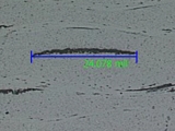
We perform a lot of material testing on coupons that are representative of the circuit board. By representative what I mean is that the coupons are designed to be on the edge of the production panel so they see the same lamination, drilling and plating as the printed wire board (PWB). The coupons contains the same geometries for hole and grid size for each type of interconnection in the product. We commonly identify four types of material damage;adhesive delamination (adhesive break-down), cohesive failure, crazing and material decomposition. Adhesive delamination is a crack that occurs between two laminated surfaces for example between B-stage (partially cured material) and C-stage (fully cured material), B-stage and copper surfaces, or between the glass fibre bundles and the resin system. Cohesive failures are exhibited as cracks within the resin but are not limited to areas where there are laminated interfaces. This type of failure may have a crack that goes through the C-stage glass bundles and extend over into the B-stage layers. Crazing is a lower-level delamination between individual glass fibres and the epoxy. The appearance of crazing looks like multiple fine silvery(fluorescing) cracks that run the length of the glass fibres. And finally material decomposition is the destruction of resin due to over heating, where the material turns black (carbonizes) and has spherical voids that confirm the resin boiled during heating. Material decomposition is typically seen where lower grade tin/lead material is exposed to a lead-free assembly and/or rework process. The photo suggests an adhesive delamination; the crack is present between two laminated surfaces. If this condition was related to the C-stage the material vendor's owns the problem. If the problem is caused by the B-stage material, it could be the PWB vendors problem. I would check the material date codes and storage conditions, to make sure the resin flow characteristics have not been violated. Also look at the lamination cycle, test temperatures (ramp rates, pressures, curing, etc.), to see if there is a reason for the delamination. This type of failure may be exacerbated by absorbed (or inherent) moisture, I would recommend baking the boards before assembly, or the thermal excursions associated with testing. I must emphasis that I have never seen delamination resolved by baking, it can be reduced on the surface layers,but not for the full construction. The bake is typically for four hours at 105 C. A longer bake than 4 hours or higher temperature tends to age the material and can make the delamination worse. To measure material degradation we design representative Interconnect Stress Test (IST) coupons that have flooded ground planes were ever they are in the product. We then measure the capacitance between the planes "as received", after simulated assembly and rework (5 or 6X230 C fortin/lead or 5 or 6X260 C for lead free) and at end of reliability testing(typically 500 cycles to 150C). A -4% change in capacitance between the readings"as received" and after the thermal excursions associated with assembly and rework, or end of test, indicates material damage was caused. We find material damage electrically rather than being limited to "hit or miss" with random cross-sections. When we find material damage in four out of six coupons (that have greater the -4% change), we micro section the failed coupons to confirm or refute whether material damage is evident.
Program Coordinator PWB Interconnect Solutions Paul Reid has over 35 years experience in bare board fabrication, quality and reliability. Working for PWB Interconnect Solutions, which does thermal cycle evaluations (IST) of representative coupons, Paul provides failure and root cause analysis of how PWBs fail. His area of expertise includes how circuit board's copper interconnections and material fails in assembly, rework and in the field, as a result of thermal cycling.
|
|||||||
| Submit A Comment | |||||||
|
Comments are reviewed prior to posting. You must include your full name to have your comments posted. We will not post your email address. |


|
Free Newsletter Subscription
Circuitnet is built for professionals who bear the responsibility of looking ahead, imagining the future, and preparing for it. Insert Your Email Address |
|
|
|
|
|
|
|
|