|
|
|
|
|
|
|
|
|
|
|
|
| Ask the Experts | |||||||
|
|||||||
|
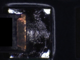
February 20, 2013 - Updated February 12, 2013 - Originally Posted Unusual Solder Appearance
D.A. |
|||||||
| Expert Panel Responses | |||||||
|
Surface effects with lead-free SAC305 can be normal. SAC305 isprone to micro-fissuring during cool down. Joints could look at times more reflective to dull, some frosty,some not. Often surface conditions are purely cosmetic and can be causedby several factors listed below.
Senior Market Development Engineer Kester Mr. Biocca was a chemist with many years experience in soldering technologies. He presented around the world in matters relating to process optimization and assembly. He was the author of many technical papers delivered globally. Mr. Biocca was a respected mentor in the electronics industry. He passed away in November, 2014.
The appearanceof the solder joint is dependent upon many variables, therefore many questionsneed to be asked relative to the appearance of that particular solder joint. My firstthought is the solderability of the solder paste. Has this been conducted? Secondly
Vice President, Technical Director EPTAC Corporation At EPTAC Corporation, Mr. Lambert oversees content of course offerings, IPC Certification programs and provides customers with expert consultation in electronics manufacturing, including RoHS/WEEE and lead free issues. Leo is also the IPC General Chairman for the Assembly/Joining Process Committee.
It'shard to say based on the photo. I see what appears to be two possible things occurring, Stress lines in the joint and component finish dissolution. I'll address the stress lines first. Stress Lines There are several things to check/compare. You can rule out the variables to hone in on the problem. Some process questions I'd pursue are:Does this only occur with one assembly, one joint / component finish or one paste type? Is this common to only one board finish? Are there any surface contaminates on the board prior to pasting / reflow? Is this a No Clean flux left on the joint? If so try removing the flux and inspect the joint finish.You may find that the joint is actually acceptable. Some other possibilities are that you may be above liquidus too long, cooling too fast or there may be board movement during the reflow process, while the joint is cooling. All of these can contribute to joint appearance and integrity. Component Finish Dissolution You may have a poor finish on your component termination. In some cases component terminations may either have minimal metalization needed to form a joint. Often the metal that is present will leach into the rest of the solder joint. This looks like what may be the case based on the color difference on the top of your component where there is less solder. To ;rule out component finish problems you can start with solderability tests. In some cases the termination may disappear leaving only the ceramic, if this is a chip. If the part passes solderability tests then the part is probably not the problem. If suspect then you can have the termination / plating evaluated at a lab which will tell you if there are problems with the base metal, contamination, composition etc.Once all variables have been ruled out you should be able to pinpoint the problem.
Sr. Manufacturing Engineer TransCore Amtech Technology Center Mr. Culpepper has over 20 years in electronic manufacturing, primarily focusing on PWA assembly.
|
|||||||
| Submit A Comment | |||||||
|
Comments are reviewed prior to posting. You must include your full name to have your comments posted. We will not post your email address. |


|
Free Newsletter Subscription
Circuitnet is built for professionals who bear the responsibility of looking ahead, imagining the future, and preparing for it. Insert Your Email Address |
|
|
|
|
|
|
|
|