I believe your answer lies in the "edge effects." The smalleraperture has an area ratio, AR(1) of 0.62. This is pretty aggressive, butprintable with good stencil manufacturing, good paste, good substrate gasketingand good process control. The longer aperture, although narrower, is mucheasier to print (AR = 0.94) because of its length.
If you look carefully at the height profile of the printeddeposits(2), you'll find that near the edges of the apertures, you have raisedpeaks of paste. This effect is greatest in corners. The peaks contribute moreto the average height measurement for small apertures, because they make up agreater percentage of the overall area of the deposit. This is especially truebecause many paste measurement systems include only the area where the pasteheight is above some threshold value.
If your paste measurement system reportsthe area of the deposits, you should notice that the deposit area is smallerthan the theoretical area of the aperture. For small apertures, this willresult in lower volume than expected, even though height may be greaterthan expected. Volume is the parameter on which you should focus, or morespecifically the transfer efficiency. Transfer efficiency is the actualdeposit volume divided by the theoretical volume of the aperture. For your300�m W by 320�m L by 127�m H aperture, I expect you will see about 70%transfer efficiency. For the 270�m W by 2050�m L by 127�m H aperture I wouldexpect a transfer efficiency of about 90%.
If your numbers are much worse thanthis, you will need to conduct focused, controlled process experiments todetermine why.- AR is defined as the ratio of aperture open area to aperture wall area
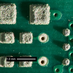
- Try viewing deposits under a stereo microscope using a point source of lightfrom a low oblique angle, perhaps 10 to 15 degrees above the horizontal. Anexample of this technique is shown in the attached photo. Notice the edge peaksand the differing shadow lengths.
Fritz Byle
Process Engineer
Astronautics
Fritz's career in electronics manufacturing has included diverse engineering roles including PWB fabrication, thick film print & fire, SMT and wave/selective solder process engineering, and electronics materials development and marketing. Fritz's educational background is in mechanical engineering with an emphasis on materials science. Design of Experiments (DoE) techniques have been an area of independent study. Fritz has published over a dozen papers at various industry conferences.
Thelikely cause is that the paste is being robbed from the slightly largeraperture / pads. It may sound strange but the best way of overcoming this andmaking the result more even would be to increase the print speed, aim foraround 30 - 70 mm/sec depending on what the paste can cope with.
Richard Boyle
Global Product Champion
Henkel Electronics
Richard Boyle is a Global Product Champion at Henkel Electronics. He has over 25 years experience in the electronics assembly industry and is responsible for the global technical service of all of Henkel's solder materials.
|