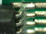
I�m not sure the exact meaning of flux exhaustion, however myinterpretation is, there wasn�t enough flux in the solder paste to prepare thepad/land area and have the molten solder flow over the complete pad or landarea itself. This would be related to percentage flux to metal ratio content ofthe paste rheology.
As for the solder paste not reflowing and appearing as thesolder balls grain structure on the surface of the solder paste, this is due tonot enough applied heat which will prevent the solder paste to become totallymolten and coalesce forming a homogeneous molten solder volume. If the solderpaste appears to not have reflowed and is as identified in IPC-A-610 section 5,the issue is that the proper intermetallic has not formed at both the componentand pad/land surface interface and this is a defective condition.
The reasoning of why it may happen on only a few pads of aparticular component is most likely due to the heat sinking characteristics ofthe pad/land area. It may be connected to inner layers of the circuit board orit may have a buried via within the pad, which is heat sinking the heat awayfrom the solder paste to make a complete solder joint.
I would suggest two issues, one review the artwork to determinethe metal load on each pad and review the thermal profile for the particularproduct being processed to verify the proper temperatures were met during thereflow cycle.
Leo Lambert
Vice President, Technical Director
EPTAC Corporation
At EPTAC Corporation, Mr. Lambert oversees content of course offerings, IPC Certification programs and provides customers with expert consultation in electronics manufacturing, including RoHS/WEEE and lead free issues. Leo is also the IPC General Chairman for the Assembly/Joining Process Committee.
It'svery hard to tell from the tiny photo, but it looks like the roughness isconfined to the solder on the land, and not so much on the joint. The key hereis whether the issue will affect the mechanical reliability of the joint. Ifthe joint is properly wetted and formed, that means there was sufficient fluxactivation to achieve the desired solder joint formation. If the shape andextent of the fillet meets the requirements, I would regard the roughness onthe solder remaining on the land as a process indicator.
Allthat said, if you are seeing this, obviously some process correction needs totake place. The first thing to do is to determine if this is really fluxexhaustion, or if it is due to insufficient temperature. A profile should tellyou right away, since flux exhaustion is due to a "too hot, too long"condition, the opposite of a too-cool condition.
Fritz Byle
Process Engineer
Astronautics
Fritz's career in electronics manufacturing has included diverse engineering roles including PWB fabrication, thick film print & fire, SMT and wave/selective solder process engineering, and electronics materials development and marketing. Fritz's educational background is in mechanical engineering with an emphasis on materials science. Design of Experiments (DoE) techniques have been an area of independent study. Fritz has published over a dozen papers at various industry conferences.
|