This type of design though not being evaluated bycomponent manufacturer either BGA/0402 but there's patent exists for same andyou can opt to try this in sample evaluation. you may google patent- US20080205011
Subrat Prajapati
Supplier Quality Leader
Ge Healthcare
Subrat has 10 year of extensive experience in PCB assembly process optimizing for quality, process includes screen printing, wave, reflow. He has a copyright in stencil design published in Apex Expo2010 at Las Vegas US.
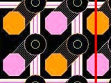
Ihave not seen this exact strategy, but it does make sense. The octagonalpattern (effectively a square with the corners cut off) provides addedclearance, vs. a square, between the lands and non-common pads while minimizingthe impact on the printing, placement and reflow processes.
It'swell documented that there is only moderate difference in printingeffectiveness between a square and a round aperture of the same dimension, andthe octagon is a "compromise" between the two. In fact, it can be shownmathematically the area ratio is exactly the same for a square, a roundaperture or an octagon of a given dimension!
The placement process should not care whether the paste deposit isrectangular or octagonal, as long as the size and spacing is correct. Thereflow process should be similarly agnostic as to shape. More important is thethermal gradient due to the interconnections with the vias. The sides of thelands attached to the (large) traces connected to the via lands will be coolerthan the opposite sides, and as a result you may see shifting of the chipsduring reflow. The traces are quite large, and I'm not sure why they need tobe.
The effect is that nearly half of the 0402 land becomes "solder maskdefined" so if the solder mask shifts relative to the metallization, the landcan grow or shrink. This effect can be minimized by reducing the trace width.You do have to be careful to maintain adequate mask web thickness to preventsolder from the 0402 from flowing down the via. A reasonable minimum is 0.003"
Fritz Byle
Process Engineer
Astronautics
Fritz's career in electronics manufacturing has included diverse engineering roles including PWB fabrication, thick film print & fire, SMT and wave/selective solder process engineering, and electronics materials development and marketing. Fritz's educational background is in mechanical engineering with an emphasis on materials science. Design of Experiments (DoE) techniques have been an area of independent study. Fritz has published over a dozen papers at various industry conferences.
|