|


|
|

| Ask the Experts | |||||||
|
|||||||
|
May 21, 2026 - Updated June 5, 2012 - Originally Posted BGA Die and Pry Testing
J.J. |
|||||||
| Expert Panel Responses | |||||||
|
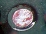
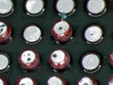
I would need more information to make the determination as to whether or not these are Kirkendall voids, as Kirkendall voids are at the intermetallic layer and this cannot be determined from these pictures. The other issue is what alloy was the solder balls on the BGA and what solder alloy was used as solder paste? The right hand pictures displays penetration of the dye around the circumference of the pad so I would guess that the pad was not completely wetted with the base solder alloy or this is where the fracturing of the solder joint started to occur. In either case more information would be needed to fully assess the situation.
Vice President, Technical Director EPTAC Corporation At EPTAC Corporation, Mr. Lambert oversees content of course offerings, IPC Certification programs and provides customers with expert consultation in electronics manufacturing, including RoHS/WEEE and lead free issues. Leo is also the IPC General Chairman for the Assembly/Joining Process Committee.
In short, I think it's unlikely that the root cause of the observed defect is Kirkendall voiding. What's needed for root cause analysis is a detailed analysis of the surface and subsurface metallurgy. Dye & pry has told you that some crack propagation has begun Perhaps not unexpected at 500 cycles. Now you need to bring the appropriate tools and methods to get to root cause. What I would do is:
Process Engineer Astronautics Fritz's career in electronics manufacturing has included diverse engineering roles including PWB fabrication, thick film print & fire, SMT and wave/selective solder process engineering, and electronics materials development and marketing. Fritz's educational background is in mechanical engineering with an emphasis on materials science. Design of Experiments (DoE) techniques have been an area of independent study. Fritz has published over a dozen papers at various industry conferences.
The amount of dye penetration looks too extensive for Kirkendall voids.Are the images showing ball separation from the chip?
President S T and S Testing and Analysis Gerald O'Brien is Chairman of ANSI J-STD 003, and Co Chairman of IPC 4-14 Surface Finish Plating Committee. He is a key member of ANSI J-STD 002 and 311 G Committees Expert in Surface finish, Solderability issues and Failure analysis in the PWA, PWB and component fields.
I don't think that it's Kirkendall voiding. It looks like poor wetting/bad adhesion. After 500 cycles it may be strain due to TCE mismatch affecting the solder (creep/fatigue failure). Do you underfill?
President, Consultant Process Solutions Consulting Inc. Lee Levine has been a Process Engineer and Metallurgist in the semiconductor industry for 30 years. He now operates his own company Process Solutions Consulting Inc where he consults on process issues and provides SEM/EDS and metallography services.
Without additional information it is difficult to be definitive on the voids shown in the picture. Kirkendall voids are typically irregular in shape and only a few microns in size, although there is no scale on the pictures these look to be much larger in size and appear to be spherical in shape. Also I would expect more of them if they were Kirkendall. It is extremely difficult to rework voids out of array components so I doubt that reworking parts will help. Finally The pictures do not appear to show die penetration in to any of the voids so the voids may not be the cause of the failure.
Senior Applications Chemist Henkel Electronics Dr. Poole is a Senior Applications Chemist in Henkel Technologies, electronics assembly materials application engineering group. He is responsible for all of Henkel's assembly products including soldering products, underfills, PCB protection materials, and thermally conductive adhesives.
While there is not enough info to make a sure call, I took your pictures and magnified them using a net camera system. I can tell you: 1)They are not Kirkendal voids. 2) The dye appears to have penetrated very little, if at all. 3)The image of the single pad shows evidence of oxidation of the copper in areas that did not wet, while some wetting did take place. 4)The image of multiple balls shows some voiding at some of the PWB pads, but not all, and some partial voids that did NOT reach down to the board pad. 5) The soldermask extends up to the edges of some of the pads, but not others, which is something I have not seen before. The only summary I have based on those two pictures alone, is that what voiding you are seeing is probably not a concern nor a reliability issue because where there are some small voids there is also very good evidence of good wetting around all of the voids, and none appear to be larger than 20% of the pad diameter. The bigger concern to me are the pads that show what appears to be oxidized copper with minimal wetting PLUS solder mask right up to the pad. This APPEARS to be evidence of oxidation, and during cycling the soldermask will actually apply tremendous pressures on the pad/solderball, causing extrusion of the solder resulting in complete separation. The reason for no dye penetration on that one? It appears you had wetting completely around the circumference of the pad, but not in large areas on the pad itself. Suggestions: Perform EDX on the both the board pads prior to assembly and those that look like the one in the picture after dye and pry. You may want to also X-ray the parts prior to assembly and reflow to see if the voids are present as received, and to what extent, just to rule them out as a cause. If the BGAs themselves show no evidence of voids or other issues, you may wish to evaluate other pastes or your paste handling system from dock to printing, but I would focus on the pad oxidation issue first with the fabricator.
Advanced Engineer/Scientist General Dynamics Richard D. Stadem is an advanced engineer/scientist for General Dynamics and is also a consulting engineer for other companies. He has 38 years of engineering experience having worked for Honeywell, ADC, Pemstar (now Benchmark), Analog Technologies, and General Dynamics.
|
|||||||
| Submit A Comment | |||||||
|
Comments are reviewed prior to posting. You must include your full name to have your comments posted. We will not post your email address. |


|
Free Newsletter Subscription
Circuitnet is built for professionals who bear the responsibility of looking ahead, imagining the future, and preparing for it. Insert Your Email Address |
|


|