It's definitelypossible that gas will be trapped and out-gas as it expands. Depending on theexact geometry of the design, this may not be a problem at all. Outgassing dueto moisture should not be a problem unless the plating in the hole iscompromised. So assuming good PWB quality, outgassing should stop at the peakreflow temperature. Any remaining gas will contract as the solder cools.Voiding may be present but most likely would not represent a reliability risk(impossible to say with certainty).The solder-bearing pin is a good way to provide the needed solder volume. Pastewould cause much more outgassing than the flux in/on the solder on the pin.
Fritz Byle
Process Engineer
Astronautics
Fritz's career in electronics manufacturing has included diverse engineering roles including PWB fabrication, thick film print & fire, SMT and wave/selective solder process engineering, and electronics materials development and marketing. Fritz's educational background is in mechanical engineering with an emphasis on materials science. Design of Experiments (DoE) techniques have been an area of independent study. Fritz has published over a dozen papers at various industry conferences.
This is the best situation seen ever and hope you will get itstabilized by conducting said methods.
1st - In order to prevent any moisture risk on Platedhole, PCB need to bake prior process.
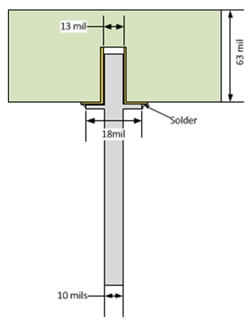
2nd - Considering all options I find the best way is toperform screen printing on Plated hole by masking hole area and opening of onlyring area on PCB where part ring will get soldered. Paste volume/thicknessshould be high eg;10-12mil paste thickness. You may need Step up stencil hereapart from regular on board SMD part soldering which can be in a single stencil.Then reflow this PCB, the paste deposited in Ring will get melted and will goinside plated hole with very less risk of air entrapment provided clearance ofplated hole to part is checked including end part of blind hole as design check.
3rd- Riskof Pin getting dis-located/tilted after reflow: To mitigate this you may needto design a top fixture to hold this part if at all you observe any such issue.
Subrat Prajapati
Supplier Quality Leader
Ge Healthcare
Subrat has 10 year of extensive experience in PCB assembly process optimizing for quality, process includes screen printing, wave, reflow. He has a copyright in stencil design published in Apex Expo2010 at Las Vegas US.
|