|


|
|

| Ask the Experts | |||||||
|
|||||||
|
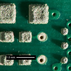
March 7, 2012 - Updated February 26, 2012 - Originally Posted Variation in Solder Paste ThicknessWe have two openings within one 5 mil laser cut stencil; one with dimension 0.32 x 0.30 and another with dimension 0.27 x 2.05. We notice that the smaller openings tend to have higher solder thickness. Our solder print system has a pressure set at 3 kg and speed of 15 mm/s. How should we go about to improve the thickness so that both openings have similar thickness? A.P. |
|||||||
| Expert Panel Responses | |||||||
If you look carefully at the height profile of the printeddeposits(2), you'll find that near the edges of the apertures, you have raisedpeaks of paste. This effect is greatest in corners. The peaks contribute more to the average height measurement for small apertures because they make up a greater percentage of the overall area of the deposit. This is especially true because many paste measurement systems include only the area where the paste height is above some threshold value. If your paste measurement system reports the area of the deposits, you should notice that the deposit area is smaller than the theoretical area of the aperture. Small apertures will result in lower volume than expected, even though height may be greater than expected. Volume is the parameter on which you should focus, or more specifically, the transfer efficiency. Transfer efficiency is the actual deposit volume divided by the theoretical volume of the aperture. For your 300um W by 320um L by 127um H aperture, I expect you will see about 70%transfer efficiency. For the 270um W by 2050um L by 127um H aperture I would expect a transfer efficiency of about 90%. If your numbers are much worse than this, you will need to conduct focused, controlled process experiments to determine why.
Process Engineer Astronautics Fritz's career in electronics manufacturing has included diverse engineering roles including PWB fabrication, thick film print & fire, SMT and wave/selective solder process engineering, and electronics materials development and marketing. Fritz's educational background is in mechanical engineering with an emphasis on materials science. Design of Experiments (DoE) techniques have been an area of independent study. Fritz has published over a dozen papers at various industry conferences.
Thelikely cause is that the paste is being robbed from the slightly largeraperture / pads. It may sound strange but the best way of overcoming this andmaking the result more even would be to increase the print speed, aim foraround 30 - 70 mm/sec depending on what the paste can cope with.
Global Product Champion Henkel Electronics Richard Boyle is a Global Product Champion at Henkel Electronics. He has over 25 years experience in the electronics assembly industry and is responsible for the global technical service of all of Henkel's solder materials.
|
|||||||
| Submit A Comment | |||||||
|
Comments are reviewed prior to posting. You must include your full name to have your comments posted. We will not post your email address. |


|
Free Newsletter Subscription
Circuitnet is built for professionals who bear the responsibility of looking ahead, imagining the future, and preparing for it. Insert Your Email Address |
|


|