|


|
|

| Ask the Experts | |||||||||||||
|
|||||||||||||
|
July 1, 2025 - Updated January 30, 2012 - Originally Posted Insufficient Plated Hole Fill with Electrolytic CapacitorsWe are having problems achieving the minimum hole of 75% on electrolytic capacitors using our wave soldering. What do you suggest? W.E. |
|||||||||||||
| Expert Panel Responses | |||||||||||||
|
You stated 75%,but you didn't say whether that is hole fill or 75% coverage of the solder source side annular ring. Fortunately you can check similar items to clear up insufficient solder problems. To achieve the 75% fill depends on a few factors. First, solderability. If the plated hole is oxidized you will have difficulty achieving proper solder joints. How long have the boards been sitting open before you attempt to process? It's possible you may need to clean the boards before you attempt to solder. See J-STD-003 for PCB solderability and IPC-CH-65B for cleaning advice. Second, Flux.Insufficient flux is another cause of insufficient solder. Whatever system you are using (bubble application, spray, ultrasonic, or proprietary application)must apply sufficient coverage to the areas being soldered. The flux also needs to be properly heated and activated to prepare the surface for soldering. Third, how is the pre-heat on your wave solder? Don't underestimate the importance of the pre-heat. Not only does the pre-heat get the flux active in preparing the surfaces, it also evaporated volatiles in the paste mix, and brings the entire assembly closer to the solder liquidus temperature. If you are attempting to solder on a multi-layer board or especially a board with an heat sink/ground plane attached to the PTH in question, pre-heat is even more critical. Finally, remember that if the PTH is connected to a heat sink or ground plane, for an IPC Class 2 assembly the criteria is 50% hole fill, not 75%.
Manager of Assembly Technology IPC Kris Roberson has experience as a machine operator, machine and engineering technician and process engineer for companies including Motorola, and US Robotics. Kris is certified as an Master Instructor in IPC-7711 / 7721, IPC A-610 and IPC J-STD 001.
What is the surface finish on the PWB, the lead to hole ratio being used and the aspect ratio/overall board thickness and how many internal planes interface are they to the through holes?
President S T and S Testing and Analysis Gerald O'Brien is Chairman of ANSI J-STD 003, and Co Chairman of IPC 4-14 Surface Finish Plating Committee. He is a key member of ANSI J-STD 002 and 311 G Committees Expert in Surface finish, Solderability issues and Failure analysis in the PWA, PWB and component fields.
We would first recommend that you assess the solderability of the board and component leads, at the same time check the hole-to-lead ratio. Too big or small it will affect the capillary effect of the solder flow. Check to see if you have a good preheat profile for the amount of flux you are using.
President/Senior Technical Consultant Foresite Mr. Munson, President and Founder of Foresite, has extensive electronics industry experience applying Ion Chromatography analytical techniques to a wide spectrum of manufacturing applications.
Have you tried high pressure? Also incorporation of voids is normally a sign that you are plating too fast.
President, Consultant Process Solutions Consulting Inc. Lee Levine has been a Process Engineer and Metallurgist in the semiconductor industry for 30 years. He now operates his own company Process Solutions Consulting Inc where he consults on process issues and provides SEM/EDS and metallography services.
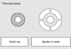
Possible cause of not reaching 75% fillet is High thermal copper layer as plane connected to capacitor PTH. Solutions-1. Design: Execute DFM on this PTH and see what is thermal value in this PTH. ie; Thermal Value = No of spokes X width of spokes XLayer Thickness, if it comes greater than 400mil Sq will sure here Design improvement is required for this you need to change PTH solid type to Spoke or web type where 4 spokes will be connected to PTH with a air gap which actually reduces thermal heat dissipation through this PTH. width of spoke will be defined by current carrying through this PTH. As shown in pic.
If your design change doesn't work out due to cost implication, try soldering through selective wave soldering with a optimized soldering parameters like time,temp or use selective wave pallet in wave soldering to execute this and optimize. Since here design is the cause mitigating with process is somewhat challenging. If this is one part, try to opt out from wave and do hand soldering with higher wattage soldering station 80W+ with Temp spec within component manufacturer recommendation.
Supplier Quality Leader Ge Healthcare Subrat has 10 year of extensive experience in PCB assembly process optimizing for quality, process includes screen printing, wave, reflow. He has a copyright in stencil design published in Apex Expo2010 at Las Vegas US.
Contributing root causes of this defect can be one or more of the following:
Process Engineer Astronautics Fritz's career in electronics manufacturing has included diverse engineering roles including PWB fabrication, thick film print & fire, SMT and wave/selective solder process engineering, and electronics materials development and marketing. Fritz's educational background is in mechanical engineering with an emphasis on materials science. Design of Experiments (DoE) techniques have been an area of independent study. Fritz has published over a dozen papers at various industry conferences.
Hole-fill is a very common issue with wave soldering and has become even more so with lead-free soldering. The cause of insufficient hole-fill is multi-faceted and can be due to several causes summarized below.
Secondly insuring the flux is applied uniformly and into the barrels to be soldered is key. This needs to be verified using thermal paper or other methods that insure the good flux penetration. The preheat has to be high enough to remove the volatiles in the flux but not too high as to cause premature de-activation of the flux.Activity is needed at the point of contact with molten solder to enhance hole-fill. To insure good hole-fill on difficult boards the immersion depth can be increased to 75% of the board thickness. Also increasing contact time at the wave can help but here you need to insure the flux is able to take the added heating. Oxidation levels of the parts to be soldered need to be understood to achieve good hole-fill. An example of difficult hole-fill would be an OSP board that saw x 2 reflow cycles prior to waving and that is relatively thick say 0.150" using no-clean ROL0 flux in a lead-free wave.Here a flux designed for difficult hole-fill assemblies would be recommendable, fluxes designed with unique activator packages, able to take slower conveyor speeds. A no-clean flux which has a slightly higher percent of solids can also help. Water washable fluxes such ORH1 are more forgiving due to their activity levels but would require complete removal of residues after soldering.
Senior Market Development Engineer Kester Mr. Biocca was a chemist with many years experience in soldering technologies. He presented around the world in matters relating to process optimization and assembly. He was the author of many technical papers delivered globally. Mr. Biocca was a respected mentor in the electronics industry. He passed away in November, 2014.
For the typical thickness sprinted circuit board, .060 and .090" boards the hole filling of the plated through holes is a matter of solderability of the surfaces to be joined. I would recommend reviewing the following conditions on the existing wave solder process as well as conducting solderability test on the components themselves. Check the requirements of IPC-J-STD-002, for the procedures for conducting solderability testing of component leads. Here are some of the issues to consider for plated through hole fill requirements.
Vice President, Technical Director EPTAC Corporation At EPTAC Corporation, Mr. Lambert oversees content of course offerings, IPC Certification programs and provides customers with expert consultation in electronics manufacturing, including RoHS/WEEE and lead free issues. Leo is also the IPC General Chairman for the Assembly/Joining Process Committee.
Solder fill is dependent on Thermal balance, lead-to-hole ratio, solder tension and cleanliness. To check thermal balance, ensure you have adequate preheat and solder temperature for your recommended alloy. Lead to hole ratio, is a function of design. You want to have better than 90% Lead to hold and possibly more if the PCB is .062 or thinner. Solder tension and Cleanliness are a function of how you process and flux type used. If you have followed recommended temperature and dwell times, your solder finish may affect this as well. There is no one answer to your question, but rather look at your soldering as a System, with dynamic variables. There might be a simple answer, but not necessarily...
Capital Equipment Operations Manager Specialty Coating Systems Rodney is currently Operations manager at SCS coatings, Global Leader in Parylene and Liquid Coating equipment. Rodney applies his BS in Computer Integrated Manufacturing from Purdue University, along with 20+ years of Electronic manufacturing and Equipment Assembly, to direct the Equipment business at SCS Coatings. "We provide unique, value added coating equipment solutions for our customers". Including conformal, spin and Parylene coating expertise.
It's really difficult to suggest something without knowing how the other components are wicking on the PCB and the solderable finish of the circuit. What I would try first THIS IS ONLY TO TEST AND DO NOT RUN LIKE THIS, but apply a small amount of flux to the topside of the PCB and flux as normal and see if this helps the wicking this would generally indicate something is lacking in the flux area if you get much better wetting. If you could supply more information then we may be able to pin point it for you.
Technical Sales Manager BLT Circuit Services Ltd Greg York has over thirty two years of service in Electronics industry. York has installed over 600 Lead Free Lines in Europe with Solder and flux systems as well as Technical Support on SMT lines and trouble shooting.
The challenging part about wave soldering electrolytic capacitors is that this cap type is a power supply filter, so the leads are connected to power planes and ground planes, most likely to internal layers of the PCB. Since the PCB is somewhat colder than the solder, these internal layers are acting like heat sinks, pulling heat out of the barrel as the solder attempts to flow up the barrel. The best designs have thermal relief for these connections between the internal planes and the power and ground pins, so less of the internal plane is directly connected to these power and ground pins. Adding a top side heater could help, but it will not completely change the dynamics. Hand soldering is an option, enough said. You can also check the requirements, since the IPC has recently been discussing changing the spec for power and ground hole fill to 50%. This is not usually to appealing to most engineers, but it is a possibility. This is one reason why there is a growing trend to reflow solder through hole components, but for electrolytics, you need to ensure the component is rated to handle the peak temperature of reflow, which for SAC305 Lead Free solder is ~ 260C for 10-20 seconds. If you are starting with a new design, and will run a new qualification process, you could also consider using a low temperature RoHS alloy such as SnBi as the alloy for reflow soldering the through hole components. Sn42Bi57.4Ag0.4 melts at138-140C, and the reflow temperature has a peak of about 180C. SMT1 and SMT2 can remain SAC305 (for example) and reflow at 240-245C, but then replace the wave process with a third reflow, using the SnBi alloy. The lower temperature third reflow will not disturb the SAC305 solder. Solder washers would likely be needed, and choosing flux coated washers is preferred.
Global Product Manager Alpha Mr. Koep is responsible for product planning and technical marketing for the Preform Products at Alpha. He is the co-author of several patents in the areas of soldering applications focusing on reflow and alternative methods.
Reader Comment
So why is a poor fill a problem, particularly for electrolytic capacitors?
Bhanu Sood, CALCE, University of Maryland, USA
Low PTH fill will typically not disrupt normal operation, but may cause temperatures to elevate in the vicinity of the PTH with the capacitor leads. The reason for the elevated temperatures is that reduced solder to PTH contact causes current crowding because the current density through these contact points can be very high. The high current densities can cause localized Joule heating which results in an elevated temperature at the contact region. In many cases the elevated temperatures may also cause localized melting and resolidification of the solder. Damage to the dielectric medium around the contact regions is also possible. In extreme cases, the leads or the cap, if displaced during a routine maintenance or handling procedure, may cause a total loss of contact with the PTH wall. Later, when the circuitry is re-energized, an instantaneous reconnection between the lead and the PTH can dissipate a lot of charge (typically through the negative lead), which is accumulated in the capacitor, and the high current creates lots of heat. The local temperature increases exponentially and surpasses the decomposition temperature of the surrounding epoxy/glass composite substrate (for FR4s). This temperature spike can also locally melt the barrel. There are recommendations on hole size, and the spec size may not always be sufficient for proper hole fill on dense components or components with large leads. The recommended hole size may be incorrect because it does not take into account board thickness and the effects of thermal load from multiple ground planes. Pin to hole ratio may be a good indicator for proper hole fill. Thermal loading (inner layer connections to the barrel) can have an effect on hole fill, the number of connected planes and more importantly, the placement of these planes (along the z) will effect thermal loads. Reader Comment
We had similar problems regarding hole fill on a large assembly in a selective wave solder process and succeeded to achieve 80 to 100% solder fill. Due to time between preheat and soldering, the preheat temperature had dropped to below minimum temperature required for proper wetting.
Frits Schoonbeek, Benchmark Electronics, Netherlands
We broke up the solder program into 3 individual parts in order to reduce the time between preheat and actual soldering avoiding too large temperature drop after preheat prior to soldering. Improving from solder fill of 20-50% to 80% or even better was achieved. Of cause previous comments addressing application of thermal reliefs in PCB design, presence of thermal planes in different layers and good solder ability of PCB and component leads are required preconditions. Reader Comment
You must make sure your top side temp is correct prior to going over the wave. Also check to make sure there is enough flux being applied.
David Morse, Whelen Engineering
Reader Comment
The above comments assumed a cool joint +/or inadequate flux. I'm assuming you have tried more flux and slower and hotter preheats. We ran into this problem and the cause wasn't too little heat, but too much heat.
Jerry Wiatrowski, General Dynamics, USA
The PTHs were not the optimum size for the small dia cap leads (PTH were too large) and the solder wetted, but then slumped back into the PTHs. We cooled down the board and got adequate fill. You can test this very easily by hand soldering a part. If it fills fine, then the assy is too hot. We found a top side temp of 100C was good for normal wave soldering. I don't recall what we had here but it was cooler. Reader Comment
I am sharing my personal experience regard to insufficient plated Hole Fill or insufficient top side filling. The PCB solderability is critical.
Poh Kong Hui, LSI-montage Service, Singapore
I used 4 different PCB vendor. One of the vendors had 100% top side filling, another vendor had about 85%. The last 2 had less than 10% top side filling. However, the last 2 had about 50% solder filling. The conclusion is that the PCB quality plays a critical role in solder filling. Reader Comment
Today's Circuit Insight addressed hole fill for capacitors. Kris Robertson replied "Finally, remember that if the PTH is connected to a heatsink or ground plane, for an IPC Class 2 assembly the criteria is 50% hole fill, not 75%."
Ed Popielarski, Technical Services, Inc.
This had changed in !PC-A-610F: Class 2 vertical fill for less than 14 leads is 75%. Capacitors have 2 leads, therefore fall into this category. 50% holds true for Class 2 for components 14 leads or more. Reader Comment
In 2015 IPC published an amendment for the 610F in which the 50% rule for Class 2 PTH's attached to a heatsinking plane where added again, next to the rule for 14 leads or more.
FRANK HUIJSMANS, PIEK
In 2017 IPC published the G Revision in which both exceptions have been included for Class 2 products. At the moment this question was raised both documents where already published. All of the experts have spoken; all have good suggestions to try. One simple method that often improves hole fill immensely is to just pre-tin the capacitor leads prior to assembly. Having solder already on the lead makes it much, much easier for the molten solder to fill the hole, even in spite of all of the other factors being present.
Advanced Engineer/Scientist General Dynamics Richard D. Stadem is an advanced engineer/scientist for General Dynamics and is also a consulting engineer for other companies. He has 38 years of engineering experience having worked for Honeywell, ADC, Pemstar (now Benchmark), Analog Technologies, and General Dynamics.
|
|||||||||||||
| Submit A Comment | |||||||||||||
|
Comments are reviewed prior to posting. You must include your full name to have your comments posted. We will not post your email address. |


|
Free Newsletter Subscription
Circuitnet is built for professionals who bear the responsibility of looking ahead, imagining the future, and preparing for it. Insert Your Email Address |
|


|