Rebecca Wheeling, Ph.D., Jeier Yang, Matt Jordan, N. Scott Bobbitt, Ben White, Mieko Hirabayashi
Sandia National Laboratories, NM, USA
Indium is used to integrate disparate semiconductor materials because of its ability to cold weld and its high ductility, even at cryogenic temperatures. Previous work used a cryogenic focus ion beam (cryo-FIB) and scanning electron microscopy (SEM) to quantify the kinetics if intermetallic growth for 3 separate underbump metallurgies (UBMs) found in literature: Thin Ti/Ni, thin Ti/Ni/Au, and thick Ti/Ni.
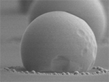
Current work seeks to better understand how the indium (In) bump size affects the respective interface kinetics and subsequent mechanical properties. Indium bumps ranging from 4-14 um were aged 1 day at 125 °C (guided by the previous results). Interfacial evolution was characterized and compared using the cryo-FIB technique. Effect on mechanical performance was evaluated by shearing as-fabricated and aged bumps. Atomistic modeling of the interface reactions, relying on density functional theory and molecular dynamics, will complement the metallurgical and mechanical analyses.
Pure indium was selected for this study because it is a commonly used single element interconnect in electronic applications that readily reacts, so it serves as a simpler case for modeling. The basis of this study will be used for board-level SnPb and Pb-free solder interconnects, where continuum modeling dominates current lifetime predictions. The eventual objective is to determine if/when interconnect sizes approach a size scale that requires atomistic considerations to maintain accurate solder behavior predictions.