Technology for Optical Co-Packaging
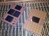
A practical approach is to use optical transceiver submodules and to attach them onto the package substrate by soldering is discussed in this paper.
DOWNLOAD
Authored By:
Yoichi Taira, Ph.D.
Keio University
Yokohama, Kanagawa, Japan
Summary
Recent advancement of information and communication technology requires high-bandwidth data transmission. Signal transmission using optical fibers is widely used because of its extremely large signal bandwidth and length product. Since the signals in VLSIs are electrical, there is always a need for EO/OE converters in a form of optical transceiver/receiver. As the required I/O bandwidth to/from VLSIs such as switch chips and CPUs increases, conventional VLSI packaging faces the I/O bandwidth bottleneck. Optical co-packaging or optical transceivers on the package is the solution, where high bandwidth data I/O is carried out without using the bottom I/O channels of the package module.
Although early examples of optical co-packaging relied on a package-on-package approach where packaged optical transceivers are socket mounted on a VLSI package, the whole package needs to be re-evaluated to support the volume demand to enable wide use of optical co-packaging such as for large-scale data-centers and 5G network. The assembly process and the long-term reliability of the components are some of the key matrices. The technology options will be discussed to realize optical co-packaging in terms of design materials and processing.
Conclusions
Technology related to optical co-packaging of VLSI is discussed. A practical approach of the optical co-packaging is to use optical transceiver submodules and to attach them onto the package substrate by soldering. Although some of the key concepts and key components were shown feasible, more detailed study of the design, process and materials is necessary. Particularly, because some surface of the package is optical path and requires protection from the environment during fabrication process, the material and package design require further investigation.
Initially Published in the SMTA Proceedings
|