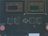
Cavity Board SMT Assembly Challenges
This study is to identifies the challenges related to assembly of a package into a cavity on the board, and establish the best known method for SMT assembly success.
DOWNLOAD
Authored By:
Dudi Amir and Brett Grossman
Intel Corporation,
OR. USA
Summary
There is a continuing trend for notebook computers, cell phones and other handheld electronic devices to become thinner and thinner. One of the solutions to reduce the thickness is mounting the tallest components into a cavity in the printed circuit board (PCB). In this method, the lands of the package that needed a height reduction are fabricated in a recess in the mother board. Paste printing and components placement take place on the surface of the board and in the cavity.
The intent of this study is to identify the challenges related to assembly of a package into a cavity on the board, and establish the best known method for SMT assembly success. The paper will examine a System-in-Package (SiP) BGA (ball grid array) package assembly into a cavity in a mother board. The paper will describe the challenges facing the PCB design and fabrication. It will share the SMT assembly method and the impact of different board suppliers, stencil technology and squeegee design. It will discuss the warpage of the PCB and its effect to SMT results. Finally, the paper will summarize the challenges and provide best known method to overcome them to have a successful assembly in a cavity board.
Conclusions
This paper describes the details of a study of assembling SiP BGA packages into a cavity. It points out the challenges involved in the board cavity design and assembly of components in a cavity.
The paper discussed the board design challenge of having a cavity and defining the proper depth of the cavity to accommodate the board fabricator, the product design, and the SMT assembly.
The paper reviewed 3D stencil technologies to allow solder print on two levels. It analyzed the pros and cons for each technology and compared their performance. There is no one selected technology which will fit all needs. The 3D stencil needs to be well designed and selected for the unique application and use.
Initially Published in the SMTA Proceedings
|