Side Wall Wetting Induced Void Formation
In this study the authors examine the mechanism of void formation in the processing of microbumps.
DOWNLOAD
Authored By:
Y. C. Liang, C. Chen, and K. N. Tu
Department of Materials Science and Engineering, National Chiao Tung University,
Hsinchu, Taiwan, R.O.C.
Department of Materials Science and Engineering, University of California at Los Angeles
Los Angeles, CA, USA
Summary
A processing failure of void formation has been observed in 3D IC microbumps due to small solder volume. We prepared the sandwiched Ni/Sn2.3Ag/Ni microbumps with 4 um and 11 um thick solders and reflowed them at 260 degrees C to study the mechanism of void formation in the processing. Due to the thin solder, intermetallic compound formation of Ni Sn from the two interfaces of the solder joint can physically bridge each other.
When that happens, the degree of freedom of motion in the direction normal to the interfaces is removed. Consequently, when the remaining molten solder is drained by side wall reaction, large voids form in the joint. This is a unique mode of processing failure because of the smaller and smaller volume of solder joints in the trend of miniaturization.
Conclusions
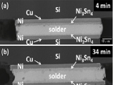
In summary, the interfacial reactions at 260 degrees C in the Ni/Sn2.3Ag/Ni microbumps with 4 im and 11 um thick Sn2.3Ag solder have been studied. The effect of small solder thickness on void formation is significant. For the 4 im thick solder, when the reflow time reached 14 min, serious necking or shrinking of the solder from the periphery was observed due to side wall wetting. After a 34 min reflow, voids formed in the center of the microbump. This is because the Ni Sn IMCs from the upper and lower interface of the microbump have bridged together, it removed the degree of freedom of the microbump to move or to shrink in the normal direction.
Hence a drain of the molten solder by the side wall wetting will leave voids in the center of the joint. This is a processing failure of the microbump in 3D IC applications. This is a unique mode of processing failure because of the smaller and smaller volume of solder joints in the trend of miniaturization. In the thicker 11 im solder, it took much longer reflow time to allow the bridging of IMC.
Initially Published in the SMTA Proceedings
|