|


|
|

| Ask the Experts | |||||||
|
|||||||
|
September 25, 2012 - Updated September 25, 2012 - Originally Posted Pin-in-Paste StandardsWhat is the recommended pin length and PTH hole dia forpin-in-paste. What is the recommended pin protrusion on the "B" side of circuit board assembly? P.K. |
|||||||
| Expert Panel Responses | |||||||
|
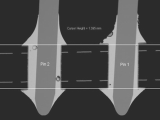
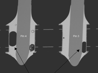
There is no "standard" per se for pin-in-paste (PiP)soldering. The closest we have is IPC-610 workmanship standard for solderjoint quality. That being said, it is often difficult to meet the samerequirements for PiP solder joints as for wave soldered joints. Pin-in-paste often results in more voids and barrel fill may be low especiallyin thick boards (<0.063in). Since through-hole part leads come invarying diameters and cross-sections, there is no one size recommendation forthe PTH. Rule of thumb dictates that less clearance of lead-to-hole isgenerally favorable for fill since it is often difficult to deposit enoughsolder paste for -610 passable solder joints. Beware reducing holediameter too drastically as outgassing solder paste fractions may result inforcible ejection of the paste or molten solder. Often PiP solder jointsdo not meet -610 requirements and a workmanship waiver may be necessary.Best to check solder joints by x-ray both laterally and normal to the boardsurface to assess vertical and circumferential fill and wetting. Remembertoo that PTH solder joints are many times stronger than SMT solder joints, sothe idea of a waiver is not unreasonable. As for lead length,there is no requirement for same since PiP does not need lead protrusion forinitial wetting as in the wave solder process. There is even a technique(Buried Intrusive Reflow - BIR) which uses a lead which is necessarily and significantlyshorter than the thickness of the PCB which makes it attractive for thick PCBs. BIR results in well-wetted, more reproducible solder joints thanconventional long-lead PiP PTH soldering and reliability studies with severalconnector styles show that it has acceptable reliability. Write to thisauthor for more information on BIR.
President Colab Engineering A thirty year veteran of electronics assembly with major OEMs including Digital Equipment Corp., Compaq and Hewlett-Packard. President of Colab Engineering, LLC; a consulting agency specializing in electronics manufacturing, root-cause analysis and manufacturing improvement. Holder of six U.S. process patents. Authored several sections and chapters on circuit assembly for industry handbooks. Wrote a treatise on laser soldering for Laser Institute of America's LIA Handbook of Laser Materials Processing. Diverse background includes significant stints and contributions in electrochemistry, photovoltaics, silicon crystal growth and laser processing prior to entering the world of PCAs. Member of SMTA. Member of the Technical Journal Committee of the Surface Mount Technology Association.
Vice President Technology Photo Stencil For over 18 years, Dr. Coleman has been the vice president of technology for Photo Stencil, working closely with customers to understand their printing requirements. His efforts have resulted in several new stencil products.
Normally you are struggling to get adequate paste volume andrequired volume increases as the square of the PTH diameter, so you really wantto minimize the PTH diameter. The minimum practical diameter is the smallestdiameter hole into which the component can be reliably inserted. Insertion iscomplicated by the fact that if you have over-printed the hole, you can nolonger see it. The lead configuration also plays a role; a lead with a taperedend is much easier to insert than one that is cut square. In general, a PTHdiameter of about 0.009" larger than the pin (either pin diameter or thediagonal measurement if it is square or rectangular) is about the smallestreliable dimension. Pin length is another matter. All depends on what the finalsolder joint requirements are: Class 3, Class 2, etcetera. If you have norequirement for visible fillets or lead protrusion on the back side, then youcan in many cases use a lead length that is equal to or even less than thetotal PWB thickness. For example, it can be very beneficial to use a leadlength that is less than the PWB thickness when working with thick boards,since the solder volume required is reduced (you need not fill the open part ofthe hole). In this case, the pin length should be long enough that the shearstrength of the soldered area of the lead surface exceeds the tensile strengthof the lead, as a general rule. In cases where visible lead protrusion isrequired, use a lead length that is equal to or only slightly greater than thePWB maximum thickness. The fillets observed on pin-in-paste joints are normallysomewhat concave, and so the end of the lead will still be visible. One major risk withpin-in-paste is failing to estimate accurately how much solder paste will fillthe PTH prior to component insertion. For small holes (<0.020" diameter) thepaste may penetrate only a short way. For large holes (>0.040") the pastemay actually fill the entire hole and be extruded out the bottom. Processcontrols are required to manage the amount of fill and avoid contaminatingtooling and equipment.
Process Engineer Astronautics Fritz's career in electronics manufacturing has included diverse engineering roles including PWB fabrication, thick film print & fire, SMT and wave/selective solder process engineering, and electronics materials development and marketing. Fritz's educational background is in mechanical engineering with an emphasis on materials science. Design of Experiments (DoE) techniques have been an area of independent study. Fritz has published over a dozen papers at various industry conferences.
|
|||||||
| Submit A Comment | |||||||
|
Comments are reviewed prior to posting. You must include your full name to have your comments posted. We will not post your email address. |


|
Free Newsletter Subscription
Circuitnet is built for professionals who bear the responsibility of looking ahead, imagining the future, and preparing for it. Insert Your Email Address |
|


|