|


|
|

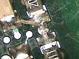
Why is Solder Dross Sticking to Our PCBAs?
Board Talk
TranscriptPhil Phil Phil Jim Some of them are not lighter than the tin lead and so they will not be skimmed off with the dross but will circulate continuously in the pot. What you are describing as dross might be other metallic contaminants other than tin and lead oxides that are not floating and are re-circulating in the pot but again, you have the core of it. You should have your pot analyzed. Phil Whether you are wave soldering, with or without dross. Jim Phil Comments
Feb 15, 2021
I have seen this before and it was mostly from the lack of flux on the surface of the PCB. Flux acts as a "Lubricant" to wash away any impurities on the board.
Ken Romer, Sr., ALTEK Electronics, Inc.
Feb 12, 2021
I had the same problem and I was scarred of dedrossing the solder pot regular as the cost to replace new solder can be high. I have used an EVS solder recovery system for many years and I clean my pot everyday. I am getting back 70% solder from my dross. Once I did this this problem went away.
Sean Williamson, Invensys
Jun 29, 2016
All comments are very good. I particularly agree with Mario regarding the negative fall on the wave flow, as we have experienced this first hand. Laminar waves with negative fall will cause exactly what you are seeing.
Ben Thomas
Jun 29, 2016
This can happen when you attempt to sweat dross in house. Up to 20% dross inclusion from this material has caused problems like this for several customers.
Mitch Holtzer, Alpha Assembly Materials
Aug 11, 2015
Check to see that your fluxer is working properly and that your preheats are bringing the board to proper temperature.
Robb Spoerri, USA
Aug 11, 2015
Might also be undercured solder mask. Fine webs of dross will stick to the porous surface. To check mask cure, get a cotton swab and some MEK. Swab the mask and if color comes off on the swab it's not properly cured.
Chrys Shea, Shea Engineering Services, USA
Jun 7, 2013
Make sure you use High Purity Tin Phos treated solder, this will stop the dross sticking to the nozzles and coming off and attaching to your PCB once the wave comes on. Poor quality solder will always do this. It is also worth periodically cleaning out the wave former to remove this powdery dross. If you cannot get to the bottom former then increase the pump speed to dislodge loose dross in the channels from the pumps. Tin/Phos again helps this dramatically. If the dross is sticking to waxy greasy residues on the PCB and you have a doughy type excess dross in your pot then check the solder resist cure.
Greg York, BLT Circuit Services Ltd, UK
Jun 7, 2013
The problem can be related to maintenance of the pump/solder pot. The pump assembly should be removed from the solder pot at least once or twice a year depending on how many hours of run time you accumulate for the pump. The dross will build up under the pump and eventually it will start going up with the solder that is pumped to create the wave. That dross will be on the surface of the wave, so when the PCB passes over the wave it will pick up dross and solder.
Julio R. Montjoy, Technical Devices Company, USA
Jun 4, 2013
The Guys are so right all none inerted waves used regularly should be de-drossed once per shift. And have a solder analysis once per quarter, this should be a Free Service from your solder supplier.
With out this information you are flying BLIND not knowing what is in your pot as the contaminates will build up with use.
Phil Tompson, EVS International, UK
Jun 4, 2013
I have seen this issue quite regularly on the wave solder, this is what happens: right after you dedross your pot, immediately after that you will see a layer of dross forming and that's ok, you will never be able to remove all the dross due to the exposure to oxygen, remember that is not recommended to dedross the pot so often you will gain nothing with these, it's always good to have a thin layer of dross since it will prevent more dross from forming.
Ok so back to the magic, once you set up the wave height to solder, you have to be very careful to set the height just at the point where there is no negative fall, that means there is no solder falling on the back of the former, so when the wave pallet or board passes through the wave it will touch the solder surface and push that thin layer of dross to the back. If you set it right you will avoid dross sticking to the board and will reduce the amount of solder bridges and insufficiences considerably. This is just the concept so if need more detail let me know, there are a whole bunch of things you need to be watching when setting up the wave solder process.
Mario Ostos, Process Engineer, Mexico
|
||||||||


|
Free Newsletter Subscription
Circuitnet is built for professionals who bear the responsibility of looking ahead, imagining the future, and preparing for it. Insert Your Email Address |
|


|