|


|
|

How To Eliminate Pesky Solder Balls?
Board Talk
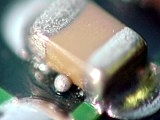
TranscriptPhil Jim Phil The best thing would be to eliminate them to begin with, that's the true remedy. Given the way these form, you're obviously using square or rectangular pads for your chip capacitors. If you examine the body of a chip capacitor where the end termination is metal, the bottom is uneven. So what happens is when the chip is placed with your pick and place machine, a certain amount of solder that is close to the inside of the pad is squeezed underneath. During reflow what happens is it is basically separated from the main mass of solder on the pad, and it forms its own little solder ball. So way you can remedy this by modifying your aperture, and hence your print shape, of the solder paste deposit for those ceramic capacitors. The most common is what is called the "home plate aperture", as it looks like a baseball home plate with the point facing towards the inside of the capacitor. You would still follow the same area, in terms of the total reduction of your aperture to be sure you're getting enough volume. There are also variations on the theme. Jim Understand, we read the questions completely, verbatim, as you send them to us. The solution that Phil and I have just proposed is universal, regardless of what kind of oven you're using, and whether it's a prototype, or a main board. It's a matter of the stencil printing, and the aperture, reducing the aperture to minimize that paste. So to wrap up, remember, don't solder like my brother. Phil Comments
Jan 6, 2015
This "solder-beading" or "squeeze-balls" as they have been termed over the years have existed a long time, as many designers create a 1-to-1 aperture-to-pad stencil design for chip components. Good comments on how to resolve from others, and kudos to Jim and Phil for revisiting, as I still have this discussion with design folks.
A little history just for fun; These always existed, but most folks used to wash boards (we still do in Aerospace) and this would remove the solder beads. With the introduction of no-clean processes, assemblers and customers did not like these beads present on the board. This and smaller chips that could easily tomb-stone, led to the introduction of the homeplate, reverse-homeplate and bow-tie apertures, eliminating solder beads and tomb-stoning. Personally I like the home-plate with points toward the component. Cheers!
Jeff Hempton, BAE Systems, USA
Sep 11, 2013
I experienced such balls due to a too high pressure on chip components with the pick and place. A too high pressure can also lead to solder beads.
Jean Michel Lasserre, SERMA TECHNOLOGIES, France
Sep 11, 2013
First of all I would say that pesky solder balls mainly generate because during the PCB design, the IPC stencil design guidelines (the latest) has not followed as Mr. Scott Homan mention, so the first action is to inform your customer or your new project development department to implement or follow the IPC stencil design guidelines to avoid or diminish as much as possible this defect in future products.
Second recommendation and as a preventive measure or general rule would be to always apply the home plate or bow-tie aperture design to all the stencils (all chip resistors and chip capacitors). I would say also that using the printing parameters to try to control the solder paste deposition to decrease the amount of paste in the pads, would not help, in my experience the main printing parameters like print speed and print pressure, has very low impact in the amount of paste you print on each pad. I would say that in order to produce some change in the conditions that produce the pesky solder ball phenomenon, the amount of paste you print must be reduced significantly. Changing the print pressure and/or print speed can not manage to reduce significantly the ammout of printed paste.
Gabriel Gutierrez S., Inventec Performance Chemicals, Mexico
Sep 11, 2013
My solutions for eliminating solder balls on Res/Cap chips are:
1. Home-plating apertures. 2. For over-sized pads, apply Bow-Tie on the land pattern recommendations. 3. For "Solder mask defined pads" 10% reduction of the aperture eliminates the excess deposit paste.
Sohrab Haddadi, M.I.S. Electronics, Canada
Sep 11, 2013
There are several reasons why we get this kind of formations after reflow. As the other comments, some due to incorrect land pattern, differences between size of the components from one supplier to another or simply an incorrect stencil aperture design.
We have seen this problem so many times and working with colleagues from the same company we have found that even we have variations between suppliers. The best option is to do a special aperture in the stencil called "inverted home base". This kind of aperture has helped us with two defects, solder balls formation and tombstoning.
Jorge Vazquez, Kostal Mexicana, Mexico
Jan 29, 2013
It is interesting that you did not comment on PCB foot prints bringing up the heal, toe and width sizes. Most PCB layout programs these days are based on the old IPC-782 footprints which were from the days of glue dots and wave soldered leaded SMT.
We have changed our libraries from IPC-782 to a modified IPC-7351 and among other advantages have seen solder balls decrease by an large amount. In general you want the PCB pad to have no more than .05mm of heal behind the actual pad so that there is no solder to squish after it.
Rick, Moog Music, Inc.
Jan 29, 2013
Root cause for this problem is not following IPC-7351 Land Pattern Standard. The heel dimension for the land should be zero, keeping the ceramic body out of the paste. The work around recipes can be found in IPC-7525 Stencil Design Guidelines. The "home plate" and "bow-tie" aperture modifications both reduce paste under ceramic. I prefer the bow-tie, it seems to help with tombstoning.
Scott Homan, IEC Electronics Albuquerque, USA
Jan 29, 2013
The first question should be whether the pads are solder mask defined or copper defined. Solder mask defined pads will certainly generate solder balls when any solder paste overlaps onto the mask which has a downward slope from covering the higher metal profile to the PCB. Copper defined pads will tend to "gather" the solder during reflow rather then disperse it. Then tweak the solder paste process.
Todd Oman, Delphi, USA
Jan 29, 2013
From my point of view, just modifying stencil design to the specific chips components and, that way, reducing solder paste deposition on pads. Also acting on paste printing parameters and, if a 3D SPI systems is available, by doing the right control of solder paste volume on the both pads.
Glayson Figueiredo, Philips Medical Systems, Brazil
Sep 13, 2010
Hey guys, Good report on those "Pesky Solder Balls". This article has been very informative. After 35 years in the industry, last Wednesday I was informed of this issue on one of our assemblies.
Fortunately I did not do the layout on this fab. But after evaluation, as you would suspect, the 805 and 603 footprints had "Oversize" pads. I will keep an eye on this. Our CM will try to limit this problem by reducing the paste stencil openings in these area's.
Tim Andrews, Bio-Rad Laboratories
|
||||||||


|
Free Newsletter Subscription
Circuitnet is built for professionals who bear the responsibility of looking ahead, imagining the future, and preparing for it. Insert Your Email Address |
|


|