|


|
|

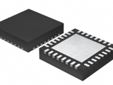
How Do You Inspect QFN Components?
Board Talk
TranscriptPhil Jim Phil Jim Or if you can extend the pads out that can help you, but to know underneath the package you need a good x-ray machine with oblique angle viewing. Top down alone is going to give you some indication, but not a really good indication of the wetting. Phil Not one of those ancient things and not one of those little cheap quickie machines. Jim Phil Jim The strategy for printing paste on that is a very complex. Most people find that some sort of window paneing gets the best coverage with the least number of defects. If you ask that question and the people look at you like you're coming from outer space, then they probably don't have much experience with QFN's. Phil I think that pretty much covers that question. Jim Phil Comments
Sep 18, 2016
Thanks to Phil and Jim for sharing this useful advice. No doubt that x-ray inspection is the most appropriate way to inspect QFN for both joints and voiding inspection. There is various type of x-ray equipment for selection in the market, example: 2D or 3D Manual, 2D or 3D Automated, In-line or Offline.
Another crucial aspect to look into is the type of voiding measurement that must be to avoid miscalculation due to x-ray image from different side of the board. Make sure you select the right equipment for your long-term manufacturing and inspection requirement. Vitrox Technologies is more than happy to share their experience and advice.
Zi Yang, Seow, Vitrox Technologies
Oct 30, 2015
Here in Komex we found a way to inspect QFNs since we don't have any Xray machine in line to verify the well soldering.
What we di is to have an over print in the 0.2 mm larger than the pad, with this solder "excess" we get a kind of chanfer on the terminals side, so we can inspect them with the angular cameras of the AOI. In regards the question from Don Patterson, in order to eliminate the solder balls, it is necessary to change the stencil aperture for those chips, try with an aperture called "inverted home base" this aperture is only for chips.
Jorge Vazquez, Kostal Mexicana
Jan 6, 2015
X-ray inspection, as per IPC-7093, and also x-section analysis for samples previously inspected and selected by x-ray images.
Glayson Figueiredo, Philips Medical Systems, Brazil
May 20, 2010
We use a bench top convection oven for prototype SMD boards. Frequently, on the sides of chip capacitors and resistors there are solder balls that must be hand removed. What's causing these to form? Also, at room temperature storage, what is the practical shelf life of a syringe of solder paste, and what symptoms would one see when the syringe is getting too old?
Don Patterson, Louisiana State University
May 19, 2010
In 2D Xray, the QFN leads look like flat strips with a dark toe. The toe is where excess solder is. The thermal pad in the center has large voids. The joint is hidden and 2D Xray is our only available tool. Can you advise further how we can judge the quality of these joints?
Ashok Dhawan, Parker Hannifin Electronic Controls, Canada
May 18, 2010
Phil and Jim, great talk and good advise! We made a study with one of our customers regarding the best pad design for automatic X-ray inspection of QFN solder joints. Feel free to contact Viscom for details!
Carsten Salewski, Viscom Inc.
|
||||||||


|
Free Newsletter Subscription
Circuitnet is built for professionals who bear the responsibility of looking ahead, imagining the future, and preparing for it. Insert Your Email Address |
|


|