|


|
|

What is the Ideal Stencil Thickness?
Board Talk
TranscriptPhil Today's question is from a Mr. or Ms. V.F. from Dallas, Texas, who writes, I have several PC boards with mixed density components. In other words, I have some of what you guys call coarse pitch, 50 mil big capacitors and the like, but I also have some difficult fine pitch, including some .5 millimeter pitch CSP's. If I use a 6-mil stencil, I have problems with my CSP's and if I go down to a 4 or 3 mil stencil, how do I get sufficient volume for the big boys? So what do I do? I'm all mixed up. Help me.
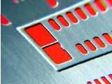
Jim Think of the other times mixed has been used. I defined mixed technology 30 years ago as printed circuit boards that have both surface bound components and through hole components on the same board. But more recently, we've talked about mixed assembly being backward and forward compatibility with lead-free assemblies, in particular backwards compatibility with lead-free components being introduced unknowingly or inadvertently into a tin lead assembly. So be careful when somebody says mixed. It's a very common word. I would have to say most boards assembled in the world today fall into this category where you have some 50-mil pitch IC's and some big capacitors which require a relatively large volume of solder. If we consider the solder fillet on the size of the leads, to get a good solder joint, you need a relatively large volume relative to the size of the pad. On the other hand, for fine pitch 20-mil pitch IC's or in this case, .5 mm pitch CSP's, they're very small leads, very small balls on the bottom of the CSP's. They need a relatively small volume of solder and solder paste to be applied in order to get the appropriate joint. What are some of our options here, Phil? Phil Jim Phil Jim What other options might we have? Phil Jim Phil And finally, another solution, and it goes under that category of everything old is new again, the old step stencil. You want to explain what a step stencil is? Jim The most common technique would be start with a thicker, in this case, 6-mil stencil, and then in the areas where you have my fine pitched parts reduce the area, usually by milling or etching the thickness of the stencil to what's required for the fine pitched part. You don't have to do any aperture reduction. You can get good fill and release and get the proper volume for the parts. Unfortunately, when you go to a step stencil, you open a whole bunch of other potential problems for design, process variables, limitations, and so forth. I think as much as we can say now. We're gonna have to come back on another session and talk about the details and trade offs for step stencils. Basically that's the problem, you have three options: thick stencil aperture reduction, thin stencil overprint, or a step stencil. Phil Jim Comments
May 28, 2017
In Asia cost is main concern. Double print is something rare here. Is step which the norm done on squeegee side can it be done on PCB side? I know some company doing it but there is no feedback what issue they encounter.
Dzulkarnain M.A
May 19, 2017
Don't forget - a number of premium stencil suppliers are now offering precision welded step stencils with none of the downsides of etch or milled steps. Welded steps have the same accuracy as the normal stainless material so can give exact paste high deposits, and they can be placed much more accurately if you have a really tight placement issue.
Fraser Shaw, Tannlin
Aug 13, 2015
For speed and accuracy, you can't beat the step stencil option. I would also recommend using nano coating. Jet printing is slow and the equipment expensive. Two print process is possible, but why do it if you can print everything at one time?
Mark Devereaux, Photo Etch Technology, USA
Jan 9, 2013
All of this skirts around what seems like the ideal solution: solder paste jet printing. The right amount of paste at every pad every time.
Lee Scanlon, Digital Monitoring Products, USA
Nov 9, 2009
These brothers by different mothers didn't even bring up the most robust solder paste print solution, i.e., a two pass screen print process. The 1st pass print would use a 4 mil thick stencil for the CSPs and ultra fine pitch ICs, etc.
The second pass print would use a 6 mil thick stencil for all other components with bottom side etch out areas over the 1st pass print component footprints. This two pass screen print process is utilized in high volume production for the 1st pass RoHS exempt high-Pb Flip Chip assembly with eutectic Sn63Pb37 solder paste, followed by the 2nd pass Pb-Free solder paste print for all other packages.
Guy Rupp, Maxim Integrated Products
Nov 9, 2009
On what basis is the stencil thickness decided in case of BGA's or fine chip components.
sudha.S, Epigon Media Technologies pvt. ltd
|
||||||||


|
Free Newsletter Subscription
Circuitnet is built for professionals who bear the responsibility of looking ahead, imagining the future, and preparing for it. Insert Your Email Address |
|


|