|


|
|

| Ask the Experts | |||||||
|
|||||||
|
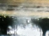
May 26, 2026 - Updated May 1, 2024 - Originally Posted Solder Ball Wrinkles
L.L. |
|||||||
| Expert Panel Responses | |||||||
|
A combination of items could cause Wrinkles with solder ball appearance post reflow
Senior Process Engineer Circuit Technology Center Brianna is a Senior Process Engineer with experience in the Medical, Semiconductor, and Aerospace & Defense industries. Proven expertise in developing and optimizing manufacturing processes while ensuring compliance with industry standards such as MIL-STD, J-STD, and IPC. Skilled in process validation, lean manufacturing, and quality improvement initiatives.
You can check section 5.2.8 (IPC-A-610) for disturbed solder and section 5.2.9 (IPC-A-610) for cooling lines/secondary reflow.
Director of Sales and Marketing Sierra Circuits Amit Bahl started to work at Sierra Circuits in 2006 where he formed strong relationships with his customers working with them on flex PCBs, HDI, controlled impedance, etc. In 2009, he was promoted Director of Sales and Marketing.
The direct answer would be, defect condition for class 2 and 3 if and only if, the total soldering system is (63/37). However, you need understand if the total system (component, solder and board finish) uses the same alloys. For example, if the BGA use 63/37, the solder pastes it’s a SAC alloy and the PADs on the PCB uses ENIG finish, the probabilities of obtaining this effect are huge. To understand this, we need to know that: The solder 63Sn/37Pb it is one of the most stable and used solders for electronics, this was because one of the principal’s characteristics it’s his eutectic point. His use is decreasing by Pb content and the ROHS regulations. In a two-component system alloy, there are several types of solid-liquid equilibrium systems. One such type, where two components of such a system are completely miscible with one another in liquid sate and they do not form any compound, on solidification they give rise to an intimate mixture known as eutectic. In a few words, this two-component system alloy 63/37, change from solid to liquid and liquid to solid only with one Celsius degree of difference. The eutectic point of the two-component system alloy 63/37 its 183 Celsius degrees. This means that at 182 degrees Celsius it is a solid, but at 183 its liquid . This characteristic is only reachable on right mixture 63/37. If the mixture change, or more than one alloy is used, the equilibrium system and characteristics of the 63/37 alloy collapse and a third state "viscous" or "pasty" appears during the transition from solid to liquid or from liquid to solid and the wrinkles can appear by slow cooling (typically effect on PBfree alloys) or vibrations/movements during solidification process. If more of one alloy are used, by mistake or by transition to PB Free. a soldering validation is required to determinate if the solder joint will be reliable.
Engineering Director / Master IPC Trainer (MIT) AMMSA Solutions More than 20 years of technical experience in the electronics industry in roles ranging from Process & Project Engineer to engineering manager and Technical Applications Engineer for Latin Americas. IPC Master Trainer, International speaker and consultant.
Wrinkles on the surface of solder balls during reflow can arise due to various factors, primarily related to the soldering process and material characteristics. Common causes include: Insufficient Flux: Inadequate flux coverage or activity can result in poor wetting of the solder, leading to the formation of wrinkles as the solder reflows. Excessive Oxidation: Oxidation of the solder surface can hinder proper wetting, causing irregularities such as wrinkles during reflow. This can occur if the solder balls are exposed to air for prolonged periods before reflow. Temperature Variation: Non-uniform heating during reflow can lead to uneven melting and flow of the solder, resulting in surface irregularities like wrinkles. Regarding the acceptability of the appearance for class 2 or class 3 products, it depends on the specific standards and requirements outlined in IPC-A-610. For class 2 products, minor surface irregularities like wrinkles may be acceptable as long as they do not compromise the functionality or reliability of the assembly. However, for class 3 products, stricter criteria are typically enforced, and wrinkles may be considered defects if they exceed specified limits or affect the integrity of the solder joint.
CTO Cybord Electronic and Mechanical Engineer with 25 years experience in technology development. CTO of Cybord, developing electronic component authentication technology using deep-tech visual inspection and big-data. Author of a book and 24 papers.
During the soldering process flux reacts with the solder oxides (oxides of Sn and Pb) and breaks them down to expose the Sn-Pb metal alloy. This is the essence of the joining process. Oxide-free solder then can wet to oxide-free bonding leads/pads. A small amount of flux should persist on the solder to keep it from re-oxidizing before the soldering process is complete. Often, in the final stages of soldering (post-temperature spike and cool-down), the hot solidifying solder will oxidize to some extent, as the last of the flux is consumed. The oxide on the solder is like a stiff shell covering the solidifying metal surface. As the solder cools, the metal alloy contracts beneath this shell. Since the inelastic oxide shell is attached to the solder and the solder is contracting during cool-down, the shell is pulled inward, and wrinkles in the oxide develop and may influence the shape of the solder beneath. Wrinkles can be seen before the solder melts, too. I have done a lot of work in terms of gaseous fluxing and have videos that clearly show this phenomenon. As for workmanship standard(s), if the solder joints meet the wetting criteria, wrinkles in the oxide shell are not be an issue. Excessive wrinkling could be a sign that the reflow profile is not appropriate for the flux, and careful inspection of the solder joints is mandated to ensure proper wetting. An appropriate reflow profile will not result in excessive wrinkling. If you care to send better photos of the issue, I’d be happy to make a more informed judgment (gratis). On my home page (link below), you’ll see a great example of ‘wrinkled’ solder.
President Colab Engineering A thirty year veteran of electronics assembly with major OEMs including Digital Equipment Corp., Compaq and Hewlett-Packard. President of Colab Engineering, LLC; a consulting agency specializing in electronics manufacturing, root-cause analysis and manufacturing improvement. Holder of six U.S. process patents. Authored several sections and chapters on circuit assembly for industry handbooks. Wrote a treatise on laser soldering for Laser Institute of America's LIA Handbook of Laser Materials Processing. Diverse background includes significant stints and contributions in electrochemistry, photovoltaics, silicon crystal growth and laser processing prior to entering the world of PCAs. Member of SMTA. Member of the Technical Journal Committee of the Surface Mount Technology Association.
I recognize this issue immediately when I see it, simply because I have been "fortunate" enough to be heavily involved in BGA reflow and rework for many years. It is possible that it is a disturbed solder condition, but far more likely it is a lack of flux on the solderball during cooldown. This same wrinkled appearance can be seen on ANY type of solder joint, not just BGA solder balls. You can re-create it simply by attempting to perform solder touchup without any flux added on any solder joint you can imagine. The good news is that you do NOT have to remove the BGA and replace it for this condition if there are no other issues seen during inspection of the BGA solder joints. What I do to fix this is to simply apply a bead of tacky flux such as Alpha WS619 which happens to be a water-soluble (my preference only, match what is on your process documentation). Heat the board up slightly in your hot air rework station (AirVac DRS or whatever you use) just enough to make the tacky flux change to a liquid, then take an air hose with just a little air pressure and blow the liquid flux underneath the BGA from all sides thoroughly such that there are no "globs" of the flux visible underneath, just a shiny coverage. Then simply reflow the BGA on the rework station using a profile that matches the initial oven reflow profile. When finished, clean thoroughly and immediately blow off the remaining moisture underneath the BGA and everywhere else. Bake dry for 20 minutes @105 C. and re-inspect. You will see clean, shiny, smooth solderballs well-wetted to the pads on both the board and the bottom of the BGA.
Advanced Engineer/Scientist General Dynamics Richard D. Stadem is an advanced engineer/scientist for General Dynamics and is also a consulting engineer for other companies. He has 38 years of engineering experience having worked for Honeywell, ADC, Pemstar (now Benchmark), Analog Technologies, and General Dynamics.
|
|||||||
| Submit A Comment | |||||||
|
Comments are reviewed prior to posting. You must include your full name to have your comments posted. We will not post your email address. |


|
Free Newsletter Subscription
Circuitnet is built for professionals who bear the responsibility of looking ahead, imagining the future, and preparing for it. Insert Your Email Address |
|


|