|


|
|

| Ask the Experts | |||||||
|
|||||||
|
July 17, 2018 - Updated January 28, 2008 - Originally Posted Improve DPPM for Wave Soldering Using NitrogenWe are wave soldering complex boards with 3000+ components using OSP finish and SAC305 alloy. Our current Defective Parts Per Million (DPPM) level for soldering is 400-500 and for solder voids is around 1000. To improve our DPPM level we plan to install a nitrogen environment around the wave soldering tank to reduce oxidation. Is this likely to improve our DPPM level? A. S. |
|||||||
| Expert Panel Responses | |||||||
|
In all probability, yes. Nitrogen will significantly reduce the amount of "air" contacting your PCB, dependent on the quality & efficiency of the equipment utilized to effect the "blanket." The question then becomes "How much of a savings will you achieve, rework Vs cost of the equipment + cost of labor + ongoing cost of nitrogen?"
President JSK Associates Based in. Northern California since 1971. Founded JSK Associates in 1979. Actively involved in soldering, cleaning, chemistries. 30 years experience in EOS/ESD control.
Highly unlikely in fact no one to my knowledgehere in the UK use Nitrogen inerting anymore. I would also not use SAC305 andOSP as the Cu dissolution would be massive. Make sure your dwell times are nomore than 2-3 seconds importantly use a good flux and ensure the alloy does nothave a gold color on the surface. Lastly make sure the solder continuallyflows over the back of the nozzle and actually flows away and doesn't gatherreducing the flow.If you want to send me some images of the defect then I maybe able to helpfurther
Technical Sales Manager BLT Circuit Services Ltd Greg York has over thirty two years of service in Electronics industry. York has installed over 600 Lead Free Lines in Europe with Solder and flux systems as well as Technical Support on SMT lines and trouble shooting.
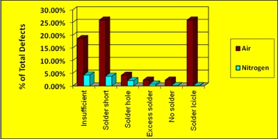
By using an inert atmosphere in the wave soldering process will reduce several defects including bridging, icicles and will improve the voiding issue. Through hole fill will also be improved. Reduction will be dependent on the O2 ppm levels and the type of inerting system that is used. Our work in this area has seen overall reduction of total defects of over 50%. Dross reduction is also a benefit that we have experienced over the years with our technology. Here is a chart that one of our customer provided on defect reduction using an inert atmosphere for SAC 305 in wave soldering.
Global Segment Manager Air Products & Chemicals, Inc. Mr. Arslanian has been involved in electronics packaging processing and equipment since 1981 including flipchip, TAB, wirebonding and die attach. Current responsiblities include R&D, applications, marketing and customer interaction.
AddingN2 to your system will help with increasing your process window but may not beworth the cost as your defect levels are pretty low. There have been numerouspapers presented on the subject of voiding with SAC in wave that requiredchanges in device lead to hole ratio changes to promote better hole fill andthus reduce the void defects - have you modified designs from when they werebuilt in SnPb or are these new designs? Secondly, how consistent is the OSPdeposit you are receiving from your board suppliers? Consistency of deposit iskey to reducing these defects - I would suggest looking at depositthickness Cpk for each of your suppliers using a non destructive measuringsystem, such as the one offered by Filmetrics. Are your supplierscontrolling the OSP process by destructive UV vis method or non destructivemicroscope methods? Are they applying the coating in a horizontal coatingsystem or in a vertical dip tank?
President S T and S Testing and Analysis Gerald O'Brien is Chairman of ANSI J-STD 003, and Co Chairman of IPC 4-14 Surface Finish Plating Committee. He is a key member of ANSI J-STD 002 and 311 G Committees Expert in Surface finish, Solderability issues and Failure analysis in the PWA, PWB and component fields.
Itwill improve but not eliminate.
SME - PWB Technologies Northrop Grumman Mahendra Gandhi has been working in interconnect industry since 1972.
It's possible that a nitrogen environment will improveperformance. It's also possible that for some defect types it will increasedefects. The nitrogen blanket will reduce the surface tension of the soldersurface, changing how it "snaps off" from component terminations and/or leads. Without specificknowledge of the design of the boards, the configuration of the wave equipment,the flux being used, etc. it's hard to say, but I think that overall a nitrogenblanket has the potential to be a benefit. Realize that you will have tooptimize the process differently once you implement. If possible, arrange tosolder some of your more difficult assemblies on a machine so equipped prior toinstalling on your machine.
Process Engineer Astronautics Fritz's career in electronics manufacturing has included diverse engineering roles including PWB fabrication, thick film print & fire, SMT and wave/selective solder process engineering, and electronics materials development and marketing. Fritz's educational background is in mechanical engineering with an emphasis on materials science. Design of Experiments (DoE) techniques have been an area of independent study. Fritz has published over a dozen papers at various industry conferences.
|
|||||||
| Submit A Comment | |||||||
|
Comments are reviewed prior to posting. You must include your full name to have your comments posted. We will not post your email address. |


|
Free Newsletter Subscription
Circuitnet is built for professionals who bear the responsibility of looking ahead, imagining the future, and preparing for it. Insert Your Email Address |
|


|